










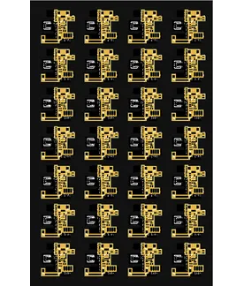
PCB Specifications
| Parameter | Value | Parameter | Value |
|---|---|---|---|
| PCB Type | Flexible PCB | Quantity | 10 pcs |
| Layers | 4 Layers | Board Type | Panel PCB |
| Dimensions | 29 x 33 mm | Copper Weight | 1/2OZ |
| Thickness | 0.23 mm | Min Track / Spacing | 6/6mil↑ |
| Surface Finish | ENIG (Immersion Gold) | Min Hole Size | 0.3mm↑ |
| Solder Mask | Black | Silkscreen | White |
| Material | Rolled Copper | Stiffener | pi,fr4 |
Manufacturing Timeline
Logistics Information
Key Manufacturing Processes
Manufacturing Summary
This order comprised ten 4-layer flex PCBs built in panel format, each measuring 29 × 33 mm with an overall thickness of 0.23 mm. The stackup utilized rolled copper at ½ oz weight, 6/6 mil trace and spacing, 0.3 mm minimum holes, black soldermask, white silkscreen, and ENIG surface finish. Both polyimide and FR4 stiffeners were selectively laminated to balance flexure zones with stable mounting areas, requiring exact registration during material preparation and coverlay processing.
We performed stackup impedance engineering and trace width compensation prior to inner layer imaging and high-pressure lamination. Subsequent steps included solder mask application, electroless nickel and immersion gold deposition, followed by TDR impedance testing, dynamic flex testing, and 100% electrical verification. The thin construction and rolled copper demanded careful polyimide handling to prevent wrinkling or delamination throughout the 22.1-day schedule.
All panels met the specified impedance values and mechanical endurance requirements, confirming consistent layer alignment and reliable long-term flex performance for this impedance controlled flexible circuit.
Explore More PCB Manufacturing Resources
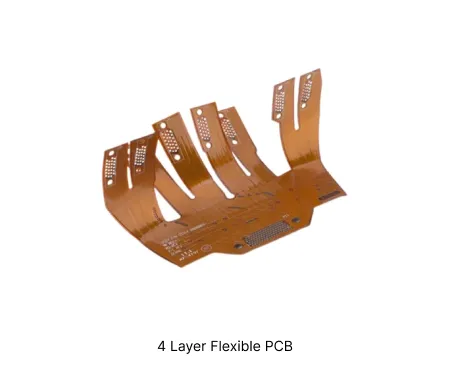
4 Layer Flexible PCB Manufacturing Insights
Discover how AIVON manufactures 4 Layer Flexible PCBs, including multilayer flexible circuit structures, layer alignment control, bending performance, manufacturing challenges, and real production experience from customer orders.
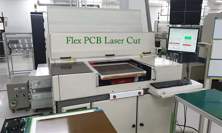
Mastering Flexible PCB Manufacturing: Handling Thin and Bendable Substrates
Learn about flexible PCB manufacturing equipment designed for handling thin, bendable substrates. Gain insights into laser cutting, adhesive bonding, and testing methods to ensure precision and reliability in production.
Real Production Records
| Order ID | PCB Type | Layers | Dimensions | Solder Mask | Surface Finish | Quantity | Action |
|---|---|---|---|---|---|---|---|
| FPC-20260821-065 | Flexible PCB | 4 | 111.25 x 16.75 | Yellow | ENIG (Immersion Gold) | 5 | View detail |
| FPC-20260819-026 | Flexible PCB | 4 | 59.8 x 65.5 | Yellow | ENIG (Immersion Gold) | 25 | View detail |
| FPC-20260810-032 | Flexible PCB | 4 | 357 x 45.8 | Black | ENIG (Immersion Gold) | 1000 | View detail |


