










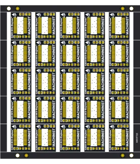
PCB Specifications
| Parameter | Value | Parameter | Value |
|---|---|---|---|
| PCB Type | FR4 PCB | Quantity | 5000 pcs |
| Layers | 2 Layers | Board Type | Panel PCB |
| Dimensions | 12 x 16 mm | Copper Weight | 1oz |
| Thickness | 1.6 mm | Min Track / Spacing | 6/6mil↑ |
| Surface Finish | ENIG (Immersion Gold) | Min Hole Size | 0.3mm↑ |
| Solder Mask | Matte Black | Silkscreen | Yellow |
| Stack-up | Custom | Impedance Control | No |
Manufacturing Timeline
Logistics Information
Key Manufacturing Processes
Manufacturing Summary
This production record covers 5000 units of 2-layer FR4 Panel PCBs measuring 12 x 16 inches, built to 1.6 mm thickness with 1 oz copper on a custom stackup. Trace width and spacing followed conventional 6/6 mil geometry while minimum hole size remained at 0.3 mm. The combination of matte black soldermask and yellow silkscreen required adjusted exposure and curing parameters to secure even coverage, sharp legend definition, and consistent color density across the large panel run.
Immersion gold ENIG surface finish was executed through electroless nickel deposition followed by controlled gold immersion, delivering flat pad surfaces essential for reliable assembly. Manufacturing progressed through engineering review, material preparation, circuit imaging and etching, solder mask application, nickel and gold plating, batch AOI inspection, and 100% electrical testing. Process parameters stayed stable throughout the 8.2-day schedule to preserve registration and plating uniformity on every panel.
The completed boards exhibited consistent dimensional stability and electrical integrity, fully satisfying the specified criteria for this high-volume panel order.
Explore More PCB Manufacturing Resources
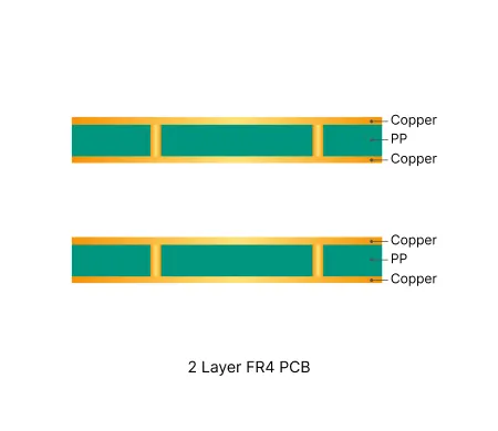
2 Layer FR4 PCB Manufacturing Insights
2 layer FR4 PCBs deliver cost-effective solutions for most electronic designs. Their simple structure enables consistent quality and efficient production cycles.
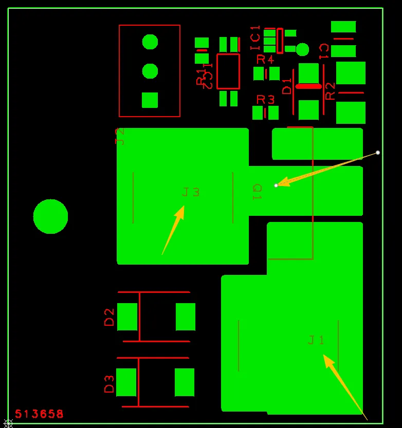
Common Engineering Queries in 2 Layer FR4 PCB Design and Manufacturing
Real Engineering Queries (EQ) and DFM issues for 2 Layer FR4 PCB (double-sided boards) from actual production reviews. Learn how to avoid common problems with via treatment, silkscreen on pads, solder mask openings, hole attributes, board edge clearance, and other frequent design pitfalls.
Real Production Records
| Order ID | PCB Type | Layers | Dimensions | Solder Mask | Surface Finish | Quantity | Action |
|---|---|---|---|---|---|---|---|
| FR4-20260910-004 | FR4 PCB | 2 | 69.92 x 69.91 | White | HASL Lead Free | 5 | View detail |
| FR4-20260907-001 | FR4 PCB | 2 | 90 x 40 | Green | HASL Lead Free | 30 | View detail |
| FR4-20260905-007 | FR4 PCB | 2 | 42.8 x 38.8 | Green | HASL Lead Free | 5 | View detail |


