










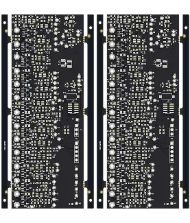
PCB Specifications
| Parameter | Value | Parameter | Value |
|---|---|---|---|
| PCB Type | FR4 PCB | Quantity | 5 pcs |
| Layers | 6 Layers | Board Type | Panel PCB |
| Dimensions | 43.75 x 116.88 mm | Copper Weight | 1oz |
| Thickness | 1.6 mm | Min Track / Spacing | 6/6mil↑ |
| Surface Finish | HASL Lead Free | Min Hole Size | 0.4mm |
| Solder Mask | Black | Silkscreen | White |
| Stack-up | Default | Impedance Control | No |
Manufacturing Timeline
Logistics Information
Key Manufacturing Processes
Manufacturing Summary
This production record details a standard 4-layer FR4 PCB run using 1.6 mm finished thickness and 1 oz copper weight across all layers. The design called for 0.3 mm minimum hole size together with 6 mil trace width and spacing, placing the geometry in conventional territory that our etching and drilling parameters handle routinely. Material preparation fed directly into inner layer imaging, circuit imaging and etching, followed by careful layer stack alignment and high pressure lamination to secure registration across the stackup.
Solder mask application preceded molten solder coating and hot air leveling, producing a consistent HASL Lead Free surface finish suited to both through-hole and surface-mount assembly. Electrical testing at completion verified continuity and isolation on every net, confirming the boards met all specified requirements without rework. The absence of impedance control or finer geometries allowed the line to maintain standard process speeds while still delivering uniform copper distribution and laminate integrity.
Completed in 2.5 days from initial engineering review to final packed panels, the order left the floor with stable thickness tolerance and clean edge definition. These execution details provide customers with multilayer PCBs that perform reliably in standard operating environments.
Explore More PCB Manufacturing Resources
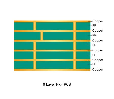
6 Layer FR4 PCB Manufacturing Insights
Six layer FR4 boards provide optimized routing density and power distribution. They require precise lamination and plating process control to maintain yield and reliability.

How to Avoid Common Engineering Queries in Multilayer FR4 PCB Design
Real multilayer FR4 PCB CAM review cases covering stack-up confirmation, impedance control, copper balance, via tenting, and edge clearance EQs. Discover practical DFM best practices for 4-layer and higher boards to reduce engineering queries, prevent warpage, and improve first-pass yield.
Real Production Records
| Order ID | PCB Type | Layers | Dimensions | Solder Mask | Surface Finish | Quantity | Action |
|---|---|---|---|---|---|---|---|
| FR4-20260911-001 | FR4 PCB | 4 | 76.33 x 49.91 | Green | HASL Lead Free | 10 | View detail |
| FR4-20260910-004 | FR4 PCB | 2 | 69.92 x 69.91 | White | HASL Lead Free | 5 | View detail |
| FR4-20260907-001 | FR4 PCB | 2 | 90 x 40 | Green | HASL Lead Free | 30 | View detail |


