











PCB Specifications
| Parameter | Value | Parameter | Value |
|---|---|---|---|
| PCB Type | FR4 PCB | Quantity | 10 pcs |
| Layers | 4 Layers | Board Type | Single PCB |
| Dimensions | 720.09 x 55.68 mm | Copper Weight | 1oz |
| Thickness | 1.6 mm | Min Track / Spacing | 6/6mil↑ |
| Surface Finish | HASL Lead Free | Min Hole Size | 0.3mm↑ |
| Solder Mask | Green | Silkscreen | White |
| Stack-up | Default | Impedance Control | No |
Manufacturing Timeline
Logistics Information
Key Manufacturing Processes
Manufacturing Summary
This 4-layer FR-4 board measured 720.09 × 55.68 mm at 1.6 mm thickness with 1 oz copper on all layers. The 10-piece order used lead-free HASL surface finish, green solder mask, and 6 mil minimum trace/space — standard geometry for this configuration. Production employed single-board format with mechanical forming and via tenting, completed within the 15-day schedule after full DFM review.
Several file discrepancies required clarification. A small gap between trace and pad was noted as intentional open design rather than defect. Via treatment showed mismatch between order requirement for cover oil and actual gerber double-sided openings, resolved by confirming process capability to minimize ink intrusion risks. Silkscreen dots at only 1 mil were flagged as unmanufacturable due to resolution limits and adjusted. Pads without openings faced potential ink coverage; these were verified against customer intent. Characters overlapping pads were reviewed for selective removal or relocation where space allowed, while factory serial number was added to the top layer. Irrelevant layers in the data were confirmed for omission.
All adjustments were implemented and re-confirmed before lamination and etching. Electrical testing verified continuity and quality on delivery. For details on the via mask window resolution and related silkscreen handling, refer to the engineering case study.
Explore More PCB Manufacturing Resources
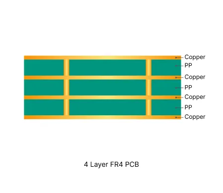
4 Layer FR4 PCB Manufacturing Insights
Standard multilayer solution offering practical routing density and controlled impedance for industrial and consumer electronics.

How to Avoid Common Engineering Queries in Multilayer FR4 PCB Design
Real multilayer FR4 PCB CAM review cases covering stack-up confirmation, impedance control, copper balance, via tenting, and edge clearance EQs. Discover practical DFM best practices for 4-layer and higher boards to reduce engineering queries, prevent warpage, and improve first-pass yield.
Real Production Records
| Order ID | PCB Type | Layers | Dimensions | Solder Mask | Surface Finish | Quantity | Action |
|---|---|---|---|---|---|---|---|
| FR4-20261009-004 | FR4 PCB | 1 | 58.85 x 65.86 | Green | HASL Lead Free | 50 | View detail |
| FR4-20261007-048 | FR4 PCB | 2 | 99.04 x 75.87 | Matte Black | HASL Lead Free | 15 | View detail |
| FR4-20261007-047 | FR4 PCB | 2 | 92.84 x 72.52 | Green | HASL Lead Free | 5 | View detail |


