










PCB Specifications
| Parameter | Value | Parameter | Value |
|---|---|---|---|
| PCB Type | FR4 PCB | Quantity | 20 pcs |
| Layers | 2 Layers | Board Type | Panel PCB |
| Dimensions | 304.74 x 422.46 mm | Copper Weight | 3oz |
| Thickness | 1.6 mm | Min Track / Spacing | 10/10mil |
| Surface Finish | HASL Lead Free | Min Hole Size | 0.3mm↑ |
| Solder Mask | White | Silkscreen | Black |
| Stack-up | Custom | Impedance Control | No |
Manufacturing Timeline
Logistics Information
Key Manufacturing Processes
Manufacturing Summary
This 2-layer FR-4 board (304.74 × 422.46 mm, 1.6 mm thick, TG150) featured asymmetric copper weights of 1 oz and 3 oz, making it a heavy copper design suitable for higher current applications. Produced as 1×4 panels for 80 pieces total with lead-free HASL finish, the order used standard 10 mil line/space, cold white solder mask, and black silkscreen. V-cut combined with routing handled separation on the large format panels.
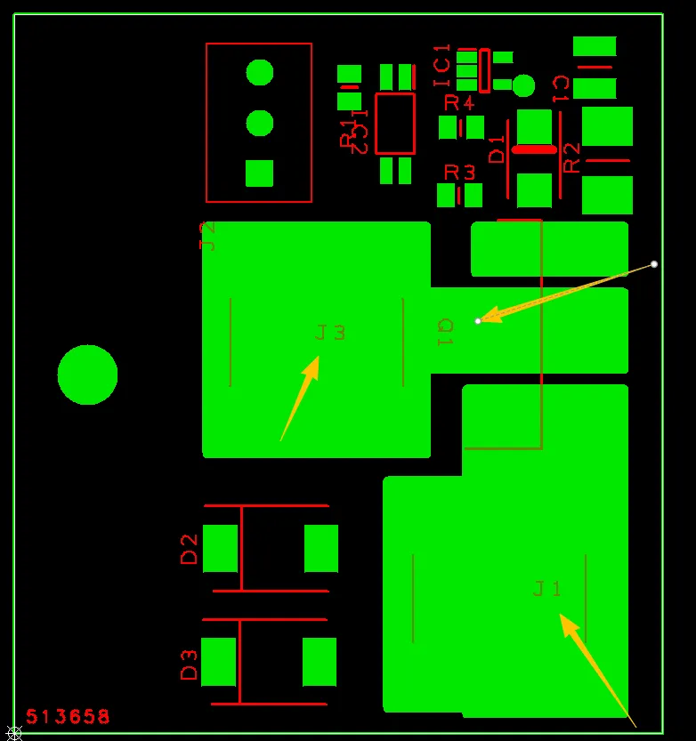
DFM review identified several execution details. Production serial number placement required location confirmation. Mismatch between upper and lower unit outlines in the panel was aligned with customer intent. Connection tabs lacked stamp holes, increasing separation difficulty, and drill tolerances for larger press-fit holes (above 2.0 mm) exceeded standard capability due to registration and tool variation. All items were clarified and adjusted before release to prevent mechanical or dimensional issues.
Panel layout and hole specifications were finalized with practical tolerances, ensuring clean routing and reliable HASL coverage on the heavy copper side. Production completed within the 5-day window with 100% flying probe testing. Full electrical test reports and quality certificates were provided with the shipment, confirming consistent board performance and assembly readiness.
Explore More PCB Manufacturing Resources
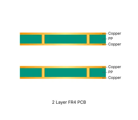
2 Layer FR4 PCB Manufacturing Insights
Discover how AIVON manufactures 2 Layer FR4 PCBs, including double-sided circuit structures, reliable through-hole fabrication processes, manufacturing challenges, and real production experience from customer orders.
Common Engineering Queries in 2 Layer FR4 PCB Design and Manufacturing
Real Engineering Queries (EQ) and DFM issues for 2 Layer FR4 PCB (double-sided boards) from actual production reviews. Learn how to avoid common problems with via treatment, silkscreen on pads, solder mask openings, hole attributes, board edge clearance, and other frequent design pitfalls.
Real Production Records
| Order ID | PCB Type | Layers | Dimensions | Solder Mask | Surface Finish | Quantity | Action |
|---|---|---|---|---|---|---|---|
| FR4-20261009-004 | FR4 PCB | 1 | 58.85 x 65.86 | Green | HASL Lead Free | 50 | View detail |
| FR4-20261007-048 | FR4 PCB | 2 | 99.04 x 75.87 | Matte Black | HASL Lead Free | 15 | View detail |
| FR4-20261007-047 | FR4 PCB | 2 | 92.84 x 72.52 | Green | HASL Lead Free | 5 | View detail |


