







PCB Specifications
| Parameter | Value | Parameter | Value |
|---|---|---|---|
| PCB Type | HDI PCB | Quantity | 5 pcs |
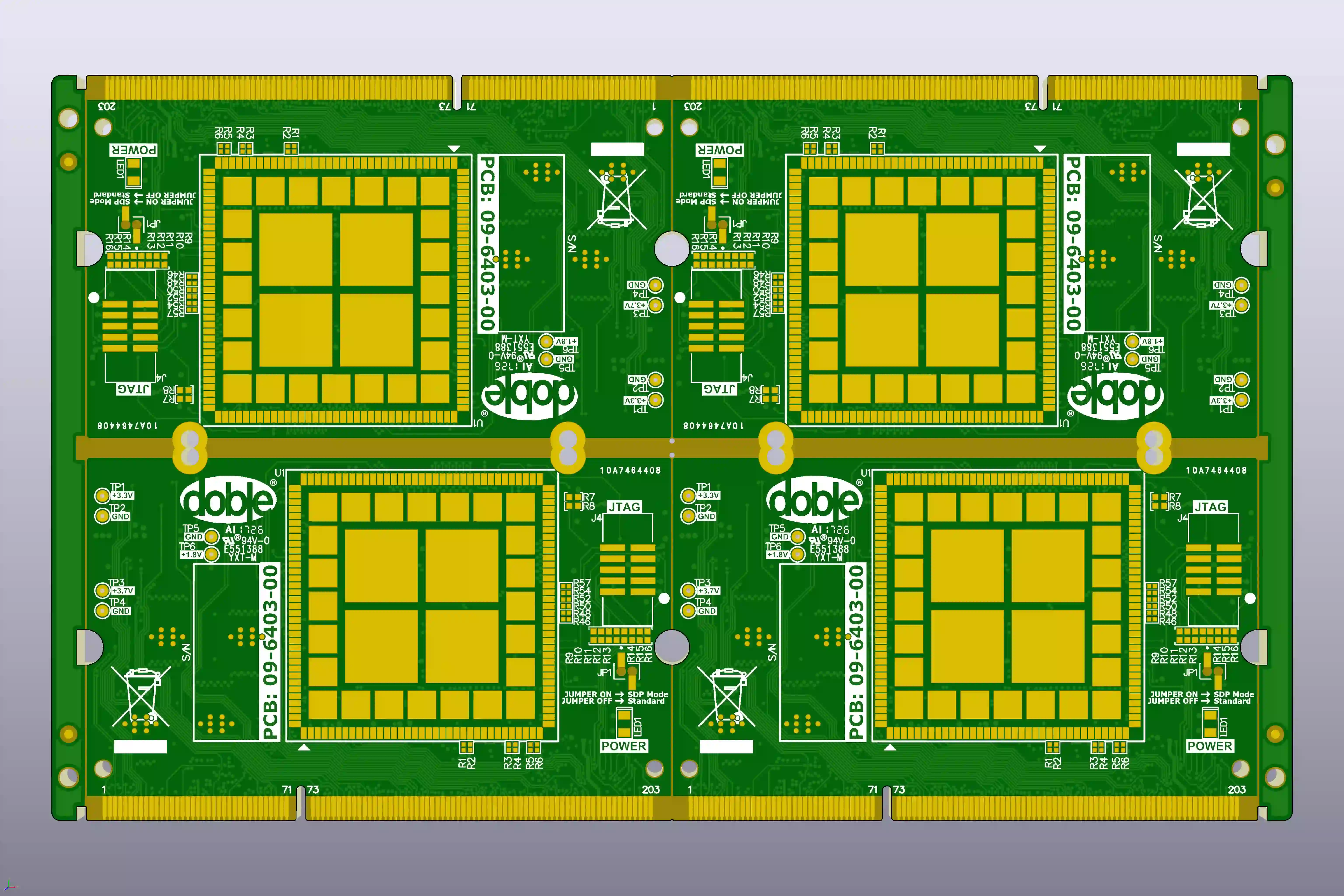
| Layers | 18 Layers | Board Type | Panel PCB |
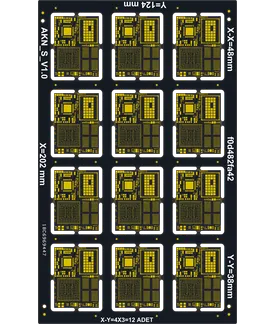
| Dimensions | 124 x 202 mm | Copper Weight | 1oz |
| Thickness | 2 mm | Min Track / Spacing | 3/3mil |
| Surface Finish | ENIG (Immersion Gold) | Min Hole Size | 0.1mm |
| Solder Mask | Matte Black | Silkscreen | White |
| HDI Structure | 3 | Blind/Buried Vias | Yes |
Manufacturing Timeline
Logistics Information
Key Manufacturing Processes
Manufacturing Summary
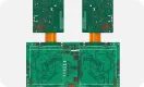
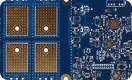
This 18-layer HDI panel PCB order required a custom stackup to accommodate its 3-step blind via structure, 3/3 mil minimum trace and spacing, and 0.1 mm holes. Produced in a quantity of five boards measuring 124 × 202 mm with 2 mm finished thickness and 1 oz copper, the design demanded exact layer registration and sequential lamination to maintain signal integrity across the impedance controlled layers.
We performed laser microvia drilling, via filling and plating, followed by matte black solder mask and immersion gold ENIG surface finish. Trace width compensation was applied during inner layer imaging and etching to achieve the tight geometries. TDR impedance testing at multiple points confirmed that the finished panels met the specified tolerances, while full electrical testing verified net continuity and isolation.
The 16-day production window allowed thorough verification at each sequential lamination stage, resulting in consistent electrical performance and dimensional stability across all delivered panels. The completed impedance controlled HDI PCBs reflect the process controls required for this advanced multilayer configuration.
Explore More PCB Manufacturing Resources
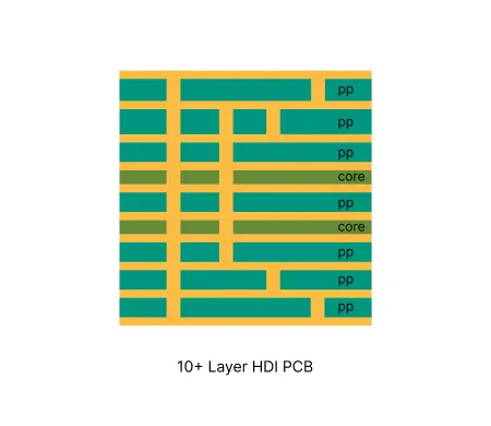
10+ Layer HDI PCB Manufacturing Insights
10+ layer HDI PCBs use sequential lamination and microvia technology to achieve high interconnect density in compact multilayer boards. Supports stacked or staggered microvias with laser-drilled structures. Compatible with high-Tg FR-4 and high-speed laminates.
How to Resolve Gold Finger Bevel and Impedance EQs in 10-Layer PCBs
Real 10-layer FR-4 case study: how CAM engineers resolved gold finger bevel clearance, impedance mismatch, tight via spacing and plugging risks to prevent scrap and signal integrity failures.
Real Production Records
| Order ID | PCB Type | Layers | Dimensions | Solder Mask | Surface Finish | Quantity | Action |
|---|---|---|---|---|---|---|---|
| HDI-20260720-0001 | HDI PCB | 8 | 188 x 100 | Matte Black | ENIG (Immersion Gold) | 125 | View detail |
| HDI-20260718-0002 | HDI PCB | 4 | 37 x 26.6 | Green | ENIG (Immersion Gold) | 20 | View detail |
| HDI-20260717-0002 | HDI PCB | 8 | 137.8 x 100.5 | Matte Black | ENIG (Immersion Gold) | 200 | View detail |


