Component Bridging
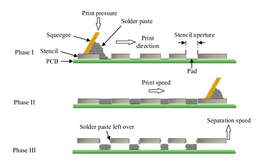
Component bridging in printed circuit board (PCB) assembly refers to the unintended formation of solder connections between adjacent pads, pins, or components, often resulting in short circuits that can compromise the functionality and reliability of electronic devices. This common defect arises during the soldering process, particularly in high-density designs where fine-pitch components are involved. Understanding component bridging is essential for engineers, technicians, and hobbyists aiming to achieve flawless PCB production, as it directly impacts yield rates, repair costs, and overall product performance. In practice, component bridging typically occurs due to factors such as excessive solder paste application, improper stencil design, or suboptimal reflow oven profiles. For instance, when solder paste bridges across pads during the reflow stage, it can create electrical shorts that lead to failures in testing or operation. To mitigate these issues, best practices include optimizing solder paste volume through precise stencil apertures, ensuring even heating in reflow processes, and incorporating design rules that increase pad spacing or use solder mask barriers. Automated optical inspection (AOI) tools also play a crucial role in early detection, allowing for quick rework before defects escalate. For those troubleshooting persistent bridging problems, articles under the Component Bridging tag offer in-depth guidance on root cause analysis, from waveform soldering techniques to advanced materials like low-residue fluxes. By applying these insights, users can enhance assembly processes, reduce waste, and improve the durability of their electronics projects. Diving into these resources provides practical strategies tailored to various PCB complexities, helping both beginners and seasoned professionals refine their techniques for consistent, high-quality results.
Technical Articles
Get in Touch
Send Message
- Products & Service
- Company
- About AIVON
- Contact
- News
- Blog
- Certification
-


- Payment
-


2026 AIVON.COM All Rights Reserved