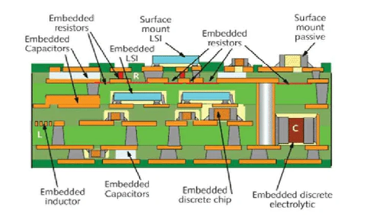
Parasitic Inductance
Parasitic inductance is an inherent phenomenon in electronic circuits and printed circuit boards (PCBs) where unintended inductive effects arise from the physical layout of conductors, such as traces, vias, and component leads. This tag encompasses a range of topics related to understanding, measuring, and mitigating these effects, which are critical for engineers and designers working on high-frequency or high-speed applications. By exploring content under the Parasitic Inductance tag, users can gain insights into how these unintended inductances can degrade signal integrity, introduce noise, or cause voltage drops in power distribution networks, ultimately affecting overall system performance. For those searching for information on parasitic inductance, this resource is particularly valuable in addressing common challenges in PCB design. Practical applications include optimizing trace routing to minimize loop areas, selecting appropriate via configurations to reduce inductive coupling, and employing decoupling capacitors strategically to counteract inductive reactance. Best practices highlighted in these articles often involve simulation tools like SPICE or electromagnetic field solvers to predict and quantify parasitic effects early in the design phase, preventing costly revisions during prototyping or production. Engineers dealing with switching power supplies, RF circuits, or digital systems will find actionable strategies to enhance efficiency and reliability, such as using ground planes to shorten return paths or incorporating ferrite beads for noise suppression. Delving deeper into the articles associated with this tag reveals case studies and tutorials that demonstrate real-world troubleshooting techniques. For instance, readers can learn how to identify parasitic inductance in oscilloscope measurements or apply formulas for calculating mutual inductance between adjacent traces. This knowledge empowers designers to create more robust electronics, ensuring compliance with standards like EMC regulations while improving product lifespan and performance. Whether you are a novice hobbyist or a seasoned professional, the content here provides the technical depth needed to tackle parasitic inductance effectively in your projects.
Technical Articles
Get in Touch
Send Message
- Products & Service
- Company
- About AIVON
- Contact
- News
- Blog
- Certification
-


- Payment
-


2026 AIVON.COM All Rights Reserved