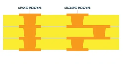
Staggered Vias
Staggered vias represent a sophisticated design technique in printed circuit board (PCB) engineering, where vias are arranged in an offset pattern rather than aligned in straight rows. This approach is particularly valuable in high-density interconnect (HDI) boards and multilayer PCBs, as it minimizes signal interference, enhances thermal management, and optimizes routing space. For engineers and designers searching for information on staggered vias, this tag serves as a centralized resource to understand their implementation and advantages in modern electronics. In practice, staggered vias help reduce electromagnetic interference (EMI) and crosstalk in high-speed circuits, making them essential for applications such as telecommunications equipment, automotive electronics, and consumer devices with compact form factors. By offsetting via placements, designers can achieve better layer transitions without compromising board integrity, which is crucial for maintaining signal quality in gigabit data rates. Best practices include calculating optimal stagger distances based on board thickness and signal frequency, ensuring compliance with manufacturing tolerances, and using simulation tools to predict performance before fabrication. These strategies not only prevent common issues like via stub effects but also contribute to more reliable and cost-effective PCB production. Professionals tackling complex PCB layouts will find detailed discussions on staggered vias throughout the articles linked here, covering topics from basic design principles to advanced integration in RF and mixed-signal systems. Whether you are refining a prototype or scaling production, these insights provide practical guidance to elevate your projects.
Technical Articles
Get in Touch
Send Message
- Products & Service
- Company
- About AIVON
- Contact
- News
- Blog
- Certification
-


- Payment
-


2026 AIVON.COM All Rights Reserved