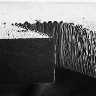
stencil-precision
Stencil precision plays a crucial role in the PCB assembly process, ensuring accurate solder paste deposition that directly impacts the reliability and performance of electronic circuits. In surface-mount technology, stencils are laser-cut or chemically etched metal foils with precise apertures that align with component pads on the board. Achieving high stencil precision minimizes defects such as bridging, insufficient paste, or misalignment, which can lead to costly rework or failures in production. For engineers and manufacturers searching for ways to optimize this aspect, understanding the factors influencing precision—such as stencil thickness, aperture geometry, and material selection—is essential. Thinner stencils, for instance, offer finer pitch capabilities but require careful handling to avoid warping, while advanced coatings can enhance paste release and extend stencil life. Practical applications of stencil precision extend to both high-volume manufacturing and prototyping environments. In automotive or aerospace electronics, where tolerances are tight, precise stencils enable consistent results across batches, supporting compliance with standards like IPC-7525. Hobbyists and small-scale assemblers benefit from best practices like using fiducial marks for alignment and calibrating squeegee pressure to prevent smearing. To improve outcomes, consider investing in nano-coated stencils for better release properties or employing automated inspection tools to verify aperture accuracy before use. Common pitfalls, such as ignoring environmental factors like humidity that affect paste viscosity, can be avoided through routine maintenance and process audits. This Stencil Precision tag gathers articles that delve into these topics, offering insights from industry experts on emerging techniques and troubleshooting strategies. By reviewing the resources here, you can refine your assembly processes and stay updated on innovations in stencil technology.
Technical Articles
Get in Touch
Send Message
- Products & Service
- Company
- About AIVON
- Contact
- News
- Blog
- Certification
-


- Payment
-


2026 AIVON.COM All Rights Reserved