uv-solder-mask
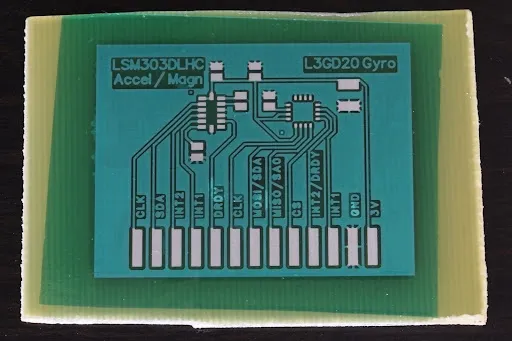
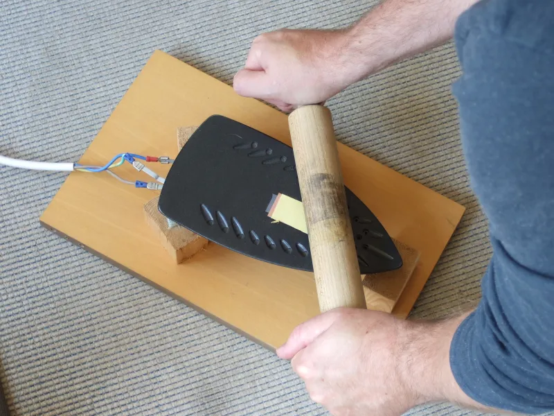
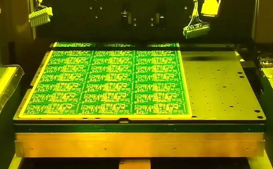
UV solder mask plays a crucial role in printed circuit board (PCB) design and manufacturing, serving as a protective coating that prevents solder bridges, shields traces from oxidation, and enhances the overall durability of electronic assemblies. This specialized material, often applied as a liquid or film, cures rapidly under ultraviolet (UV) light, offering advantages over traditional thermal curing methods such as faster production times and greater precision in high-volume environments. For engineers, hobbyists, and technicians searching for information on UV solder mask, this tag aggregates resources that delve into its composition, application techniques, and compatibility with various PCB substrates. Understanding these fundamentals can help you select the right mask for your project, whether you are prototyping a simple circuit or scaling up for commercial production. In practical terms, UV solder mask provides actionable benefits like improved insulation and resistance to environmental factors, making it ideal for applications in consumer electronics, automotive systems, and aerospace components. Best practices include ensuring even application to avoid defects such as bubbles or incomplete coverage, using appropriate UV exposure times to achieve optimal hardness, and integrating it with silkscreen processes for clear component labeling. Users often seek guidance on troubleshooting common issues, such as mask adhesion problems on flexible PCBs or color variations for aesthetic purposes. Articles linked under this tag offer step-by-step tutorials on DIY application methods, comparisons with other mask types like epoxy or liquid photoimageable options, and tips for integrating UV curing equipment into your workflow. By exploring the content here, you can gain insights into emerging trends, such as eco-friendly UV mask formulations that reduce volatile organic compounds, and how they align with modern sustainability standards in electronics manufacturing. This knowledge equips you to make informed decisions, optimize your PCB designs, and avoid costly errors in assembly.
Technical Articles
Get in Touch
Send Message
- Products & Service
- Company
- About AIVON
- Contact
- News
- Blog
- Certification
-


- Payment
-


2026 AIVON.COM All Rights Reserved