










Fast PCB Prototyping: Bring Your Ideas to Life
Key Moment
What This Video Covers
This video explores how fast PCB prototyping turns engineering concepts into functional hardware quickly and reliably. Aivon specializes in helping engineers and OEM teams move from idea to working prototype with minimal delays, supporting everything from simple single-layer designs to complex multilayer configurations.
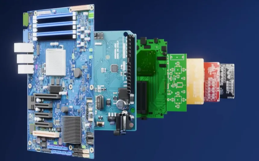
The video covers Aivon's quick-turn PCB manufacturing capabilities, including 1-32 layer boards using materials such as FR4, aluminum, flexible circuits, and rigid-flex PCB constructions. It highlights how rapid prototyping services help teams validate signal integrity, thermal performance, and mechanical reliability before committing to full production.
Whether you're developing medical devices, automotive electronics, IoT products, or industrial control systems, fast PCB prototyping reduces iteration cycles and de-risks new product development. The process emphasizes quality-focused fabrication, precise layer stack-up control, and dependable turnaround times that engineering teams can trust.
Get an instant PCB quote to see pricing for your next prototype. For projects requiring component assembly, explore our turnkey PCB assembly services. Teams working with flexible designs can also request a flex PCB quote or rigid-flex PCB quote.
Key Highlights
- Quick-Turn Capability: Fast PCB prototyping from 1 to 32 layers with support for FR4, aluminum, flex, and rigid-flex technologies to match diverse engineering requirements.
- Accelerated Iteration: Reduce product development cycles by transforming ideas into testable prototypes with reliable manufacturing processes and material options.
- Engineering-Focused Service: Designed for OEM engineers and procurement teams needing dependable quality, material versatility, and scalable support from prototype to production.
Quick-Turn Capabilities Across Layer Counts and Constructions
Fast PCB prototyping covers single-sided and double-sided boards through complex 32-layer constructions. Standard FR4 remains the most common substrate for general digital and mixed-signal designs, while aluminum (metal-core) boards address thermal dissipation needs in power and LED applications. Flexible circuits based on polyimide and rigid-flex combinations support dynamic or space-constrained form factors.
Lead times typically start at 24–72 hours for simpler designs and extend to 5–7 days for high-layer-count or rigid-flex builds, depending on copper weight, via technology, and surface finish. Fabrication maintains tight registration, controlled dielectric thickness, and reliable plating to ensure the prototype behaves like the eventual production board.
Material Options Supporting Diverse Engineering Requirements
Material selection directly influences electrical performance, mechanical durability, and thermal behavior. FR4 grades with controlled dielectric constant and loss tangent suit most digital and analog circuits. Aluminum-core laminates improve heat spreading and reduce component temperature rise. Polyimide flex materials provide repeated bend capability, while high-performance laminates support higher-frequency or higher-reliability rigid-flex constructions.
Proper material choice at the prototype stage prevents later redesigns caused by unexpected impedance variation, excessive warpage, or thermal failure. Stack-up documentation that specifies core and prepreg thicknesses, copper weights, and glass styles allows fabricators to maintain consistent electrical and mechanical results across builds.
Accelerating Iteration While Controlling Manufacturing Risk
Each prototype cycle that returns accurate, reliable boards shortens overall development time. Teams can confirm schematic correctness, layout integrity, and system-level behavior before committing to tooling or volume material purchases. Quality-focused processes—including automated optical inspection, electrical testing, and controlled lamination cycles—reduce the chance that manufacturing artifacts mask design issues.
When component assembly is required, integrated SMT services deliver fully populated boards ready for functional testing, further compressing the validation loop.
Critical DFM Considerations for Fast PCB Prototyping Success
Successful quick-turn fabrication depends on design decisions made before files are submitted. Controlled impedance traces require accurate dielectric thickness and copper weight data in the stack-up; deviations of only a few microns can shift characteristic impedance outside specification and produce reflections or timing errors. Via aspect ratios should remain within fabricator capability limits—typically 8:1 or lower for standard processes—to avoid plating voids that create intermittent opens under thermal cycling.
Panelization and breakaway methods affect both yield and mechanical stress on the finished board. Scoring or routing that leaves insufficient edge clearance can induce copper lifting or delamination during depaneling. For aluminum-core boards, the metal thickness and dielectric isolation layer must be specified clearly; inadequate thermal interface or mismatched expansion coefficients lead to warpage and solder-joint fatigue.
Flex and rigid-flex designs demand attention to bend radius, coverlay openings, and transition zones between rigid and flexible sections. Sharp corners or abrupt thickness changes concentrate stress and initiate cracks in copper or coverlay during flex testing. Early DFM review that flags these issues before fabrication begins prevents the most common causes of prototype failure and subsequent redesign.
Layer Count, Lead Time, and DFM Focus Guide
| Layer Count | Typical Lead Time Range | Primary Material Options | Key DFM Focus Areas |
|---|---|---|---|
| 1–2 | 24–72 hours | FR4, aluminum | Trace width/spacing, copper balance |
| 4–8 | 3–5 days | FR4, high-Tg FR4 | Impedance control, via aspect ratio |
| 10–16 | 5–7 days | FR4, specialty laminates | Registration, lamination pressure |
| 18–32 | 5–10 days | High-performance FR4 | Stack-up symmetry, resin fill |
| Flex / Rigid-Flex | 5–10 days | Polyimide, adhesiveless | Bend radius, coverlay adhesion |
Common Production Challenges and Proven Mitigation Approaches
Even with correct design data, manufacturing variables can introduce defects. Insufficient resin flow during lamination of high-layer-count boards may leave voids that later expand under thermal stress and cause delamination. Uneven copper distribution produces local warpage that complicates assembly and can crack solder joints. In flex circuits, incomplete adhesive coverage or moisture absorption before lamination leads to blistering or coverlay lift.
Mitigation begins with balanced copper pours, proper use of thieving patterns, and moisture-control protocols for polyimide materials. Fabricators that maintain documented process windows for press cycles, plasma desmear, and plating chemistry consistently reduce these failure modes. Electrical test coverage that includes net continuity and isolation, combined with cross-section analysis on first-article boards, confirms that the physical product matches the design intent before functional testing begins.
Surface-finish selection also affects both assembly and long-term reliability. HASL may be acceptable for simple prototypes, but ENIG or immersion silver provides flatter surfaces and better fine-pitch performance when the prototype will later move to production.
Industry Applications and Validation Outcomes
Medical device teams use fast PCB prototyping to confirm biocompatibility-compatible materials and signal integrity under strict regulatory timelines. Automotive electronics groups validate thermal and vibration performance of multilayer and aluminum-core boards before design freeze. IoT and industrial control developers rely on rapid flex and rigid-flex iterations to refine form factors and interconnect reliability.
In each case the ability to obtain consistent, production-representative boards within days rather than weeks allows earlier detection of layout or component issues and reduces the probability of costly late-stage changes.
FAQ
Q1: How long does fast PCB prototyping typically take at Aivon?
A1: Aivon offers quick-turn PCB prototyping services, with standard lead times starting from 24-72 hours for simple designs and up to 5-7 days for complex multilayer or rigid-flex boards, depending on specifications.
Q2: What materials are available for fast PCB prototyping?
A2: We support FR4, aluminum (metal core), polyimide-based flexible materials, and high-performance laminates suitable for rigid-flex constructions, high-frequency applications, and standard industrial use.
Q3: Can I get PCB assembly together with my fast prototype order?
A3: Yes. Aivon provides integrated PCB assembly and SMT services alongside prototyping, allowing you to receive fully assembled boards for immediate testing and validation.
Q4: What DFM checks are performed before a quick-turn job is released to production?
A4: Automated and manual DFM screening verifies minimum trace/space, annular ring, copper balance, drill-to-copper clearance, and solder-mask expansion. Any violation that would cause scrap under accelerated processing is flagged for correction before panels are committed.
Q5: How does board thickness or copper weight affect fast prototyping schedules?
A5: Boards thicker than 2.0 mm or copper heavier than 2 oz require slower drill feeds and extended etch times. Staying within 1.6 mm and 1 oz copper on the first prototype preserves the shortest possible cycle; heavier constructions are best introduced after the design has been functionally confirmed.
Every great product starts with a prototype.
From 1 to 32 layers, we support a wide range of materials — standard FR4, aluminum, flexible and rigid-flex substrates or more options.
Controlled impedance, fine-pitch routing, blind and buried vias, and multiple surface finishes are all available at prototype quantities — so you can test the exact stackup and performance you need.
Every file is checked automatically and reviewed by engineers to confirm stackups, clearances, and manufacturing rules before production begins.
During fabrication, your boards go through AOI, flying-probe testing, and full process traceability, ensuring they arrive fast and perform reliably in real evaluation.
Whether you're verifying a new concept or preparing for a production build, our prototype service delivers consistent results — with fewer surprises and quicker iteration.
Turn your PCB idea into a real board — faster, easier, and more reliable.





