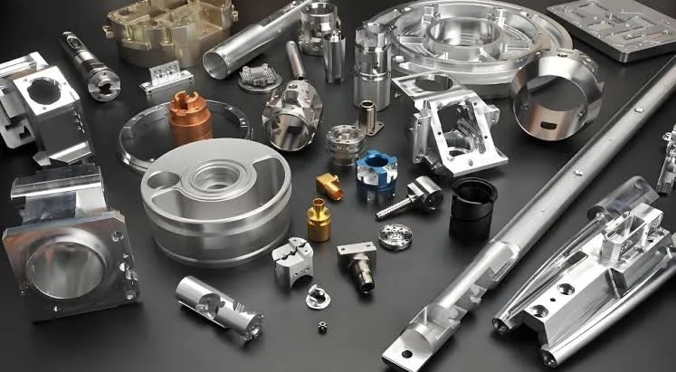
Poor PCB enclosure thermal design shows up fast in production. Components run hotter than expected, sometimes right at the edge of spec, because the heat path from board to metal case never quite works as drawn. In CNC machined enclosures, this is especially common. The rigid metal and tight tolerances look perfect on paper, but small layout decisions destroy the thermal interface.
Why Component Heat Rarely Reaches the Enclosure Wall
Engineers often place high-power parts near the board edge thinking the machined aluminum case will act as a giant heatsink. Then they rely on a few mounting screws or simple pressure contact. In practice the actual contact area ends up tiny. Air gaps of 0.1–0.3 mm kill conduction.
CNC machining leaves surface flatness variations. Typical flatness on a 100 mm span might sit around 0.05–0.15 mm depending on the alloy and fixturing. Add board warp, tolerance stack on standoff heights, and thermal interface material compression, and you get inconsistent pressure across the contact zone.

Thermal Resistance Jumps Quickly With Small Gaps
A 0.1 mm air gap has thermal resistance orders of magnitude higher than direct metal-to-metal or TIM contact. Heat from a 5 W regulator barely moves into the enclosure. Junction temperatures climb 20–40 °C above predictions. We see this repeatedly in DFM reviews.
Heatsink Placement That Ignores Enclosure Contact
Many layouts bolt a heatsink directly to the PCB and assume the enclosure will help. Without deliberate thermal paths from heatsink base to case, the benefit stays limited to local convection inside the box. The CNC machined enclosure stays cool while the board cooks.
The fix requires planning copper pours, thermal vias, and contact pads that line up with enclosure bosses or flat surfaces. Designers often forget to coordinate the mechanical drawing with the PCB layout early enough.
Mounting Hole and Boss Alignment Problems in PCB Enclosure Thermal Design
Screw holes placed without considering thermal paths create point loads. The board flexes slightly under torque and lifts away from the enclosure surface elsewhere. Heat spreading copper on the bottom layer never makes reliable contact.
Typical CNC tolerance on boss height and location runs ±0.1 mm. PCB fabrication tolerance on hole position is similar. Stack them up and you easily lose flat contact over a 20 mm pad area. Thermal interface materials need uniform pressure to perform. Without it they behave like insulators in spots.
Common Via Pattern Mistakes Under Thermal Pads
Filled and capped vias help, but many designs use standard thermal reliefs or too few vias. Heat gets bottlenecked at the copper-to-via transition. For serious dissipation we want via arrays on 1–1.5 mm pitch with 0.3 mm or larger drilled holes, plugged and plated over.
Leaving the vias open invites solder wicking during assembly and creates uneven surfaces that worsen enclosure contact. Production teams see this often.

Material and Surface Finish Effects on Long-Term Thermal Performance
Anodized enclosures look nice but add thermal resistance. Bare machined aluminum or chemical conversion coating transfers heat better. Many overlook this when selecting finishes for EMI reasons.
Over time, oxidation and thermal cycling degrade the interface. Without proper TIM or thermal grease that stays in place, contact resistance rises. We recommend specifying gap-filling compounds rated for the expected temperature range and vibration environment.
Tolerance Analysis Most Layout Tools Miss
Worst-case stack-up calculations rarely include thermal expansion differences. Aluminum expands more than FR-4. At operating temperature the board can bow away from the enclosure bosses. This opens the critical gap exactly when you need conduction most.
Spring-loaded contacts or compressible TIM with higher thickness tolerance help here. Rigid metal-to-metal designs need careful analysis of operating temperature deltas.
Layout Adjustments That Actually Improve PCB Enclosure Thermal Design
Start by marking enclosure contact zones on the mechanical drawing and transferring them to the PCB layout as keep-in areas. Place large copper pours on the bottom layer aligned with these zones. Add thermal vias directly under hot components leading to those pours.
Keep the copper area at least 2–3 mm larger than the component thermal pad to account for misalignment. Use multiple mounting screws around high power sections to maintain pressure. Avoid running traces that force component placement away from optimal contact points.
For critical designs, consider stepped cavities in the CNC enclosure or dedicated thermal bosses machined to tighter flatness. This costs more but beats field failures.
Assembly and DFM Checks That Catch Thermal Path Issues Early
During DFM we always ask for the enclosure 3D model or at minimum the critical dimensioned drawing. Checking component heights against internal clearance and contact areas prevents surprises. Boards with tall parts near contact zones often need relief pockets machined into the case.
Specify flatness requirements on the PCB drawing for areas intended for thermal contact. Standard FR-4 twist and bow tolerances can exceed 0.75% of diagonal – enough to break contact on larger boards.
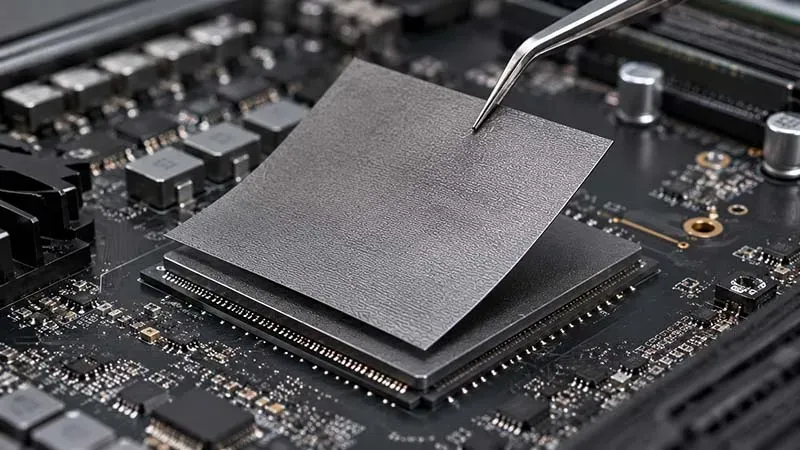
Thermal interface materials need defined compression. Call out the exact type and thickness. Production teams can then verify torque specs on screws to achieve consistent pressure without cracking the board.
Testing Reality Versus Simulation
Simulation assumes perfect contact. Real hardware shows higher temperatures until you iterate the mechanical interface. IR imaging during prototype testing reveals the actual hot spots and poor transfer areas quickly. Fix them in layout before release.
Pay attention to edge effects. Heat spreads laterally in copper but drops off fast without enclosure contact. Larger copper areas help but only when the enclosure path is solid.
Key Takeaways for Better PCB Enclosure Thermal Design
Treat the enclosure as an active part of the thermal system from the start. Align high dissipation components and their copper pours with machined contact surfaces. Account for real manufacturing tolerances instead of ideal CAD models. Use adequate via arrays and proper TIM selection.
Small layout changes early prevent big thermal problems later. The difference between a marginal design and a reliable one often comes down to a few millimeters of contact area and proper via planning.
Review the mechanical and PCB files together before finalizing routing. It takes time but saves far more in prototyping and field returns. Good PCB enclosure thermal design is mostly about consistent physical contact and heat spreading paths that survive assembly variation.