Fiber optic patch cords and LiFi visible light communication systems are critical enablers of high-speed, low-latency data transmission in modern networks. While fiber optics handle long-haul and high-bandwidth backbone links, LiFi delivers wireless connectivity through visible light. Both technologies ultimately depend on printed circuit boards that manage electrical-to-optical conversion, signal integrity, thermal dissipation, and long-term reliability under demanding operating conditions.
Fiber Patch Cord Types and Mode Conversion on PCB Platforms
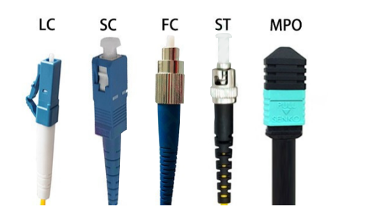
Fiber patch cords are classified by fiber type—single-mode (OS1/OS2) and multimode (OM1–OM5)—and by connector style, including LC, SC, MPO/MTP, and specialized mode-conditioning cords. Mode conversion is required when connecting single-mode and multimode segments or when upgrading legacy infrastructure to higher-speed transceivers.
On the PCB level, these connections interface with optical transceiver modules and mode-conversion circuits. High-speed SerDes lanes on switch and server line cards demand controlled-impedance differential pairs, back-drilled vias, and low-loss laminates to preserve eye diagrams during electrical-to-optical transitions. Mode-conditioning patch cords translate to PCB layout constraints: precise fiber alignment features, integrated mode scramblers, and thermal vias beneath laser drivers or photodetectors to maintain wavelength stability. High-Tg FR4 or Rogers-based hybrid stack-ups ensure minimal insertion loss and return loss across 10G, 40G, 100G, and 400G Ethernet ports.
LiFi Visible Light Communication and PCB Implementation Requirements
LiFi uses LED luminaires for downlink and infrared or visible-light photodetectors for uplink, achieving multi-Gbps speeds with inherent physical-layer security. The technology requires precise modulation of LED current, fast photodetector response, and robust ambient-light rejection.
From a PCB perspective, LiFi transceivers integrate high-current LED driver ICs, transimpedance amplifiers, and baseband processors on the same substrate. Thermal management becomes critical: heavy copper planes, embedded copper coins, and arrays of thermal vias dissipate heat from high-power LEDs without compromising signal integrity. Controlled-impedance routing and EMI shielding cages prevent interference between the optical front-end and digital processing sections. High-frequency laminates with low dielectric loss support the multi-GHz modulation bandwidths required for 5G/6G backhaul or industrial wireless links.
Unified PCB Manufacturing and Reliability Considerations
Both fiber-optic and LiFi systems share common PCB requirements. Sequential lamination with laser-drilled microvias enables dense routing around optical connectors and fine-pitch BGA packages. Filled and capped vias eliminate stubs that degrade high-speed signals. Rigorous impedance control (±5% tolerance) and automated optical/X-ray inspection guarantee consistent performance across production batches.
Aivon's manufacturing capabilities support these applications through hybrid material stack-ups, advanced thermal via technology, and high-reliability processes tailored for optical and wireless communication hardware.
Future Trends in PCB Technology for Optical and Visible-Light Systems
Next-generation fiber and LiFi deployments are driving several PCB technology advances. Co-packaged optics and linear pluggable optics require HDI PCBs with embedded optical engines and sub-100 µm dielectric layers to minimize conversion loss. LiFi systems are moving toward 10 Gbps+ per channel, necessitating ultra-low-loss laminates and integrated liquid-cooling channels directly beneath LED arrays.
Sustainability trends favor halogen-free, high-Tg materials with improved recyclability, while AI-driven impedance monitoring and real-time thermal sensing on the board itself enable predictive maintenance in both fiber and LiFi networks.
Conclusion
Fiber patch cord mode conversion and LiFi visible light communication deliver complementary high-speed connectivity solutions, yet their performance hinges on the underlying printed circuit boards. Through optimized stack-up design, impedance control, thermal management, and precision manufacturing, engineers can meet the stringent electrical, optical, and thermal requirements of these technologies.
Aivon's expertise in high-reliability HDI, hybrid-material construction, and rigorous signal-integrity validation positions the company as a trusted partner for delivering the advanced PCBs that power next-generation optical and visible-light communication systems.