Satellite internet and non-terrestrial network (NTN) voice services are transforming global connectivity by extending high-speed broadband and reliable voice communication to remote, maritime, aviation, and disaster-stricken regions. At the core of these systems lie specialized printed circuit boards that must withstand extreme radiation, thermal cycling, vibration, and long propagation delays while delivering the signal integrity, power efficiency, and miniaturization required for spaceborne payloads, ground gateways, and user terminals.
Satellite Internet Architecture and PCB Integration Points
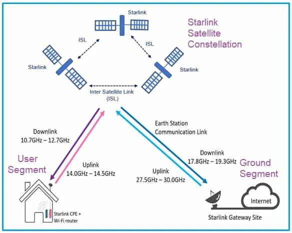
A typical satellite internet system comprises three segments: the space segment (constellations of low-Earth-orbit satellites), the ground segment (telemetry, tracking, control stations, and gateways), and the user segment (terminals and handsets). Each segment imposes distinct PCB requirements.
In the space segment, satellite payloads perform high-speed signal processing, beamforming, and power amplification. These functions demand multilayer PCBs with precise impedance control, high-frequency laminates, and robust via structures to maintain signal integrity across wide bandwidths. Ground gateways interface satellite links with terrestrial fiber networks; their PCBs must support dense I/O, high-current power planes, and EMI shielding to prevent interference between uplink and downlink paths. User terminals, including handheld NTN devices, rely on compact HDI PCBs that integrate RF front-ends, baseband processors, and power management within tight size and thermal budgets.
Enabling NTN Voice: PCB-Level Challenges and Solutions
Voice services over IoT NTN introduce additional constraints. Propagation delays, limited air-interface bandwidth, and the need for low-latency call setup require PCBs that minimize signal path length and optimize power delivery. Three key bearer types—data, voice signaling, and voice media—must coexist on the user-plane, often necessitating dynamic bearer management implemented through high-reliability interconnects and controlled-impedance routing.
To reduce signaling overhead, designers employ simplified IMS SIP flows. This optimization translates directly to PCB layout: shorter trace lengths, reduced via counts, and strategic placement of codec and gateway functions on the same substrate to cut round-trip latency. Low-rate voice codecs further lower bit-rate demands, allowing thinner copper layers and smaller vias while maintaining thermal performance in power amplifiers.

Material Selection and Stack-Up Strategies for Satellite Environments
Reliability in space and high-altitude environments dictates material choices. High-Tg FR4 or specialized polyimide laminates resist thermal expansion mismatch during orbital temperature swings. Controlled dielectric constants and low-loss tangents preserve signal integrity at millimeter-wave frequencies used in modern constellations. Copper thickness is increased on power planes to handle high-current demands of phased-array antennas, while heavy copper or embedded metal cores improve heat spreading from high-power RF components.
Via technology is equally critical. Microvias and via-in-pad constructions enable the dense routing required for HDI satellite modems. Filled and capped vias prevent outgassing in vacuum and maintain mechanical integrity under launch vibration. For NTN handsets, sequential lamination with laser-drilled vias supports the transition from terrestrial 5G to satellite fallback without compromising board thickness or warpage.
Thermal Management and EMI/EMC Design in Communication PCBs
Satellite payloads and NTN terminals generate significant heat in compact enclosures. Effective thermal vias, copper pours, and heat-spreader layers integrated into the PCB stack-up keep junction temperatures within specification. EMI shielding—achieved through via fences, embedded ground planes, and selective conformal coatings—protects sensitive receive chains from self-interference and external radiation.
In NTN voice applications, Doppler shift and phase noise must be managed at the board level. Stable clock distribution networks with low-jitter routing and dedicated power domains for oscillators directly improve voice quality and call success rates.
Manufacturing Processes and Reliability Assurance
High-reliability satellite PCBs undergo rigorous fabrication controls. Sequential lamination, laser drilling, and plasma etching ensure via reliability under thermal cycling. Automated optical inspection, X-ray, and electrical testing verify impedance and continuity across thousands of nets. For space-qualified boards, additional outgassing, vibration, and thermal-vacuum testing confirm performance before integration.
Aivon's manufacturing capabilities support these requirements through advanced HDI, heavy-copper, and hybrid-material stack-ups tailored for telecommunication and aerospace customers. Controlled impedance, via-fill processes, and high-Tg materials enable the compact, high-performance boards essential for next-generation satellite constellations and NTN voice handsets.
Future Trends and Design Implications
As constellations scale to tens of thousands of satellites and NTN voice becomes mainstream, PCB technology will continue to evolve. Standardized modular payloads, reusable launch vehicles, and direct-to-device 5G NTN handsets will drive demand for even denser interconnects, advanced thermal interfaces, and radiation-hardened laminates. Integration of satellite and terrestrial networks will require PCBs that seamlessly support dual-mode operation while meeting stringent size, weight, power, and cost targets.
By focusing on signal integrity, thermal dissipation, material stability, and manufacturing precision at the PCB level, engineers can unlock the full potential of satellite internet and NTN voice services. Aivon continues to collaborate with communication-system integrators to deliver the high-reliability boards that form the backbone of these critical infrastructures.