Electronic enclosure design mistakes show up as higher quotes, longer lead times, and unexpected rework. Most problems start in the CAD model and only become expensive after the first articles arrive. These are the issues that repeatedly drive cost in sheet metal and machined enclosures.
Wrong Material Selection Early in the Design
Choosing stainless when aluminum would meet the requirements is a classic cost driver. Material price is only part of the problem. Harder alloys slow machining, increase tool wear, and complicate forming.
Match the material to the real environment. Indoor equipment rarely needs the corrosion resistance of 316 stainless. Starting with the lowest-cost alloy that still works keeps the entire process simpler.
Overly Complex Geometry That Forces Extra Operations
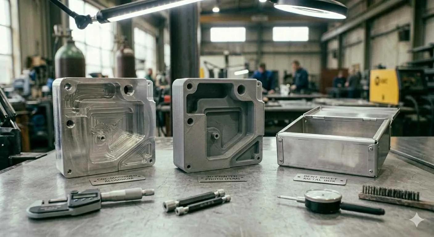
Deep pockets, undercuts, and non-standard radii look good on screen. In production they require special tooling, multiple setups, or secondary machining. Each added operation multiplies cost.
Keep features within standard tool and brake capabilities. Simple forms almost always cost less and ship faster.
Ignoring Sheet Metal Bend Limitations
Bend radii smaller than material thickness, flanges too short for the tool, or features too close to the bend line create scrap or force hand work. These electronic enclosure design mistakes are easy to catch in the model but expensive after laser cutting.
Use the shop’s minimum bend radius and flange length guidelines from the start. Most fabricators publish them.
Unrealistic Tolerance Stack Across the Enclosure
Calling ±0.1 mm on every dimension when ±0.25 mm is acceptable raises inspection time and reject rates. Tight tolerances on large sheet metal parts are especially costly because of spring-back and thermal effects.
Reserve tight tolerances for critical interfaces — mounting holes for the PCB, connector cutouts, and mating surfaces. Leave the rest open.
How Tolerance Choices Affect Secondary Operations
When primary dimensions are too tight, the shop often adds grinding or secondary machining just to meet the print. That cost was never in the original estimate.
Poor Hole and Cutout Placement
Holes too close to edges or bends cause distortion. Oversized or undersized connector cutouts force rework. Patterned ventilation holes without proper spacing can leave the part too weak for handling.
Keep holes at least 2× material thickness from edges and bends. Verify connector footprints against actual hardware, not just datasheet drawings.
Designing Without Assembly Sequence in Mind
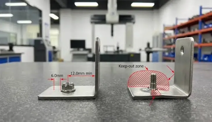
Enclosures that cannot be assembled without temporary fixtures or special tools drive labor cost. Blind fasteners, inaccessible screws, and tight internal clearances create the same problem.
Model the full assembly early. Check tool access for every fastener and verify that the PCB can be installed and removed without binding.
Insufficient EMI Shielding Provisions
Leaving gaps at seams, using non-conductive coatings on critical interfaces, or omitting gasket grooves forces later fixes. Conductive gaskets, finger stock, or secondary plating then become expensive add-ons.
Design continuous metal contact paths from the beginning. Specify conductive finishes only where needed and leave clear notes for the fabricator.
Inadequate Thermal Paths and Ventilation
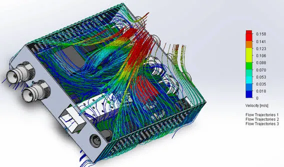
Sealed boxes without heat sinking or airflow force the addition of fans, larger heat sinks, or material changes after the first thermal test. These late changes are always more expensive than designing the path correctly the first time.
Identify the highest power components early and provide direct metal contact or deliberate airflow channels. Simple features added in the original design cost far less than redesigns.
Late Discovery of Fit and Finish Issues
Parts that look correct in CAD but do not assemble cleanly create the highest rework costs. Tolerance stack, spring-back, and coating thickness are the usual culprits.
Build a prototype or at least a fit-check model before releasing production files. Catching interference early prevents the most expensive electronic enclosure design mistakes.
Practical Ways to Reduce Enclosure Cost in Design
Use standard material thicknesses and bend radii. Limit critical tolerances to functional interfaces. Design for the fewest setups possible. Confirm EMI and thermal requirements before locking geometry.
A short DFM review with the fabricator before release catches most of these issues. The time spent early is almost always cheaper than the rework that follows a flawed design.
Clean, practical enclosure design keeps manufacturing cost under control and reduces the chance of late surprises. That is the real goal of avoiding these common mistakes.