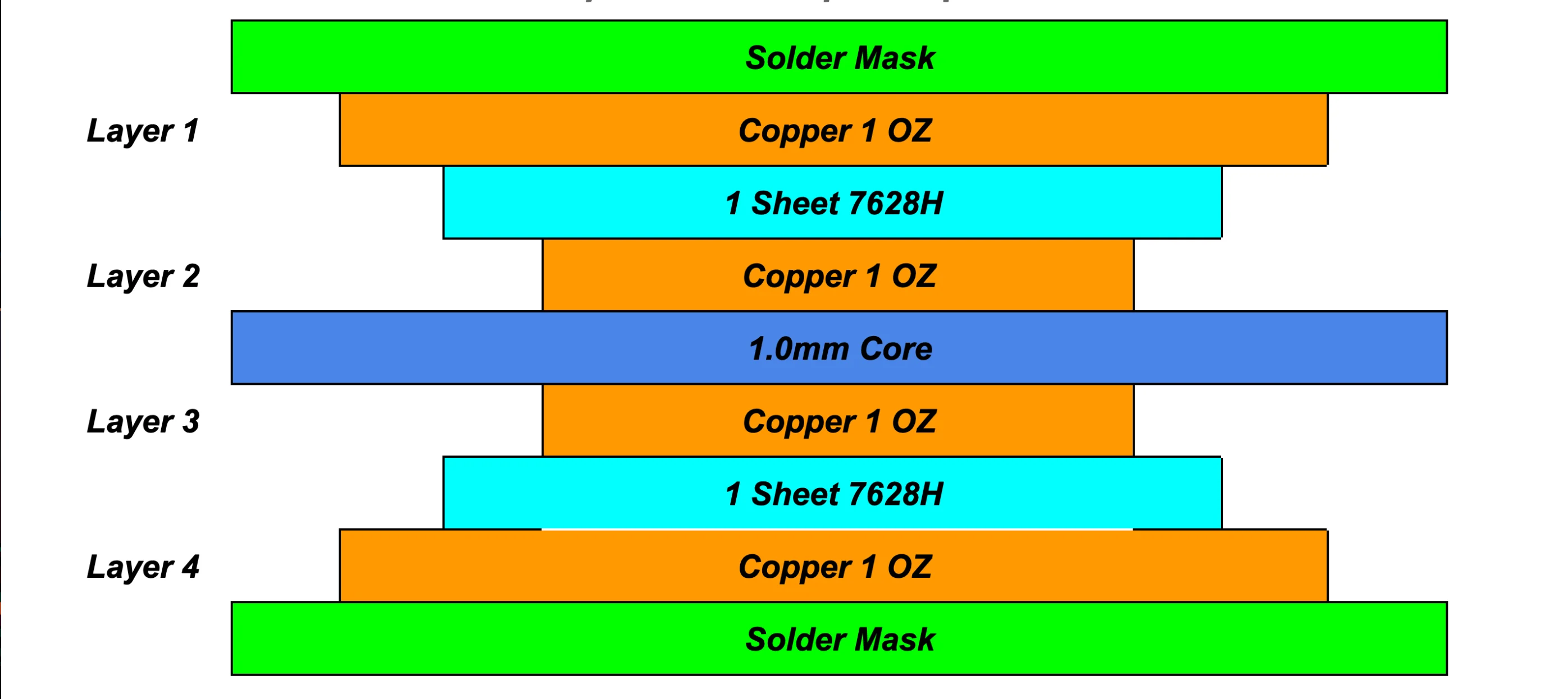
During CAM review of a 2-layer FR-4 panel measuring approximately 212 mm by 582 mm, our engineering team identified pads positioned too close to the board outline. This Pad to Outline Clearance concern immediately raised the risk of copper exposure after contour routing. From a DFM perspective, the primary concern was manufacturing stability and long-term edge reliability rather than whether the design could simply be fabricated. Without clarification, the finished boards could have entered assembly with exposed copper along the edges, creating potential short-circuit and corrosion pathways.
The order ( #FR4-20260416-075 ) specified TG150 material, 1.6 mm thickness, 1 oz copper on both sides, matte black solder mask, white silkscreen, lead-free HASL, and customer-supplied panelization using scoring. Quantity was 15 sets. These parameters are common, yet the combination of a large panel format, zero process edge, and tight pad-to-outline distances required careful verification before release to production.
Why This Large-Panel Design Triggered Detailed Edge Clearance Checks
Our CAM engineer first examined the Gerber outline and copper layers against the supplied fabrication notes. The panel was customer self-panelized into eight units with scoring separation and no process edge. In this configuration, the contour routing tool path runs directly along the final board perimeter. Any copper feature that approaches or crosses the defined outline risks being cut through or left with insufficient solder-mask coverage after milling.
Further measurement confirmed that multiple pads sat closer to the outline than the safe clearance typically required for reliable contour routing on 1.6 mm FR-4. At the same time, the connection ribs between boards lacked stamp holes, and the requirement to add a production number plus date code carried no specified location. These secondary observations compounded the overall risk picture, but the pad-to-outline distance remained the dominant manufacturability issue.
Risk indicators included the absence of a process edge, the use of scoring rather than routing with tabs, and the relatively large panel dimensions. On a long, narrow panel the cumulative tolerance stack-up of scoring and final contour can easily consume the remaining clearance, leaving copper exposed.
| Feature Observed | Measured Condition | DFM Concern |
|---|---|---|
| Pad-to-outline distance | Insufficient on multiple locations | Copper exposure after contour |
| Connection ribs | No stamp holes present | Handling and depanelization stress |
| Production marking | Location unspecified | Potential interference with copper or mask |
Table 1: summarizes the key observations that triggered the Engineering Question.
Pad to Outline Clearance Risks That Could Not Be Overlooked
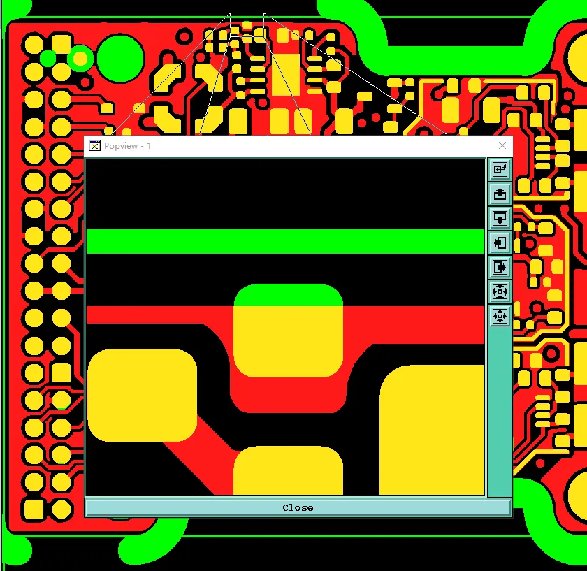
The most significant risk was copper exposure after contour routing. When a pad or copper feature lies too close to the board edge, the milling cutter removes part of the copper or leaves a thin residual that is easily damaged. On a lead-free HASL finish the exposed edge copper is especially vulnerable to oxidation and solder-mask undercut.
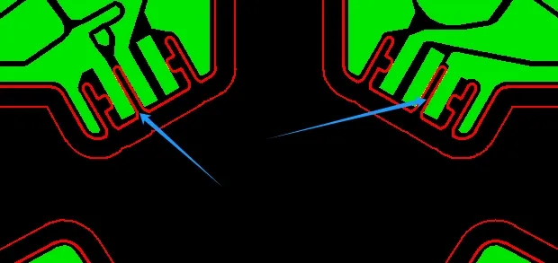
Figure 1: the pad in the file is too close to the outline
A second risk involved the missing mouse bites on the connection ribs. Without these holes the ribs remain solid copper or laminate bridges that must be broken by force during depanelization. The resulting stress can propagate micro-cracks into adjacent copper or solder-mask areas.
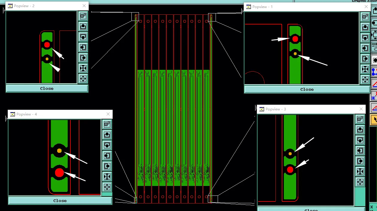
The third observation concerned the production number and date-code placement. Because the fab drawing required these markings yet gave no coordinate, an operator could inadvertently locate them on copper features or too near the edge, creating additional clearance violations or cosmetic defects.
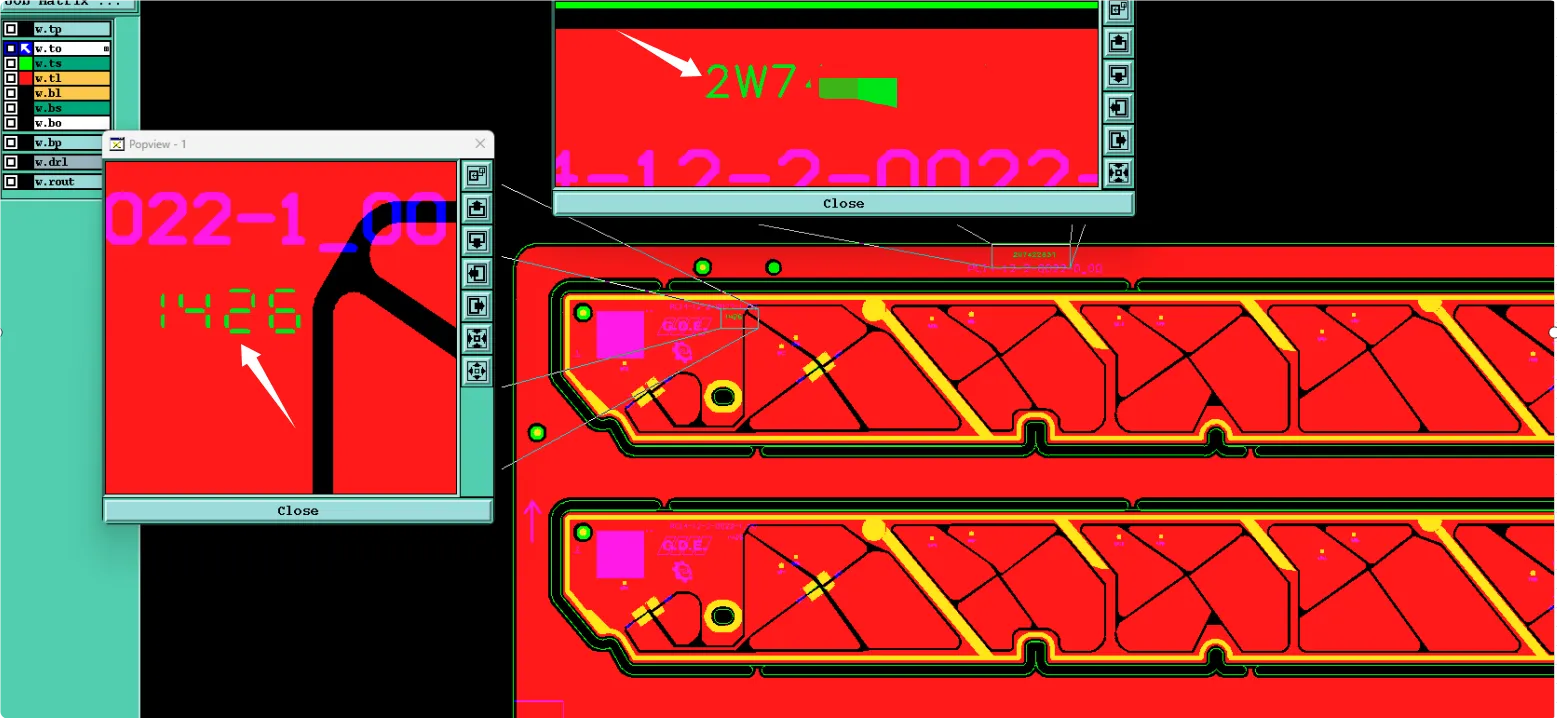
Figure 2: add the date code and production NO. in the arrow part area
From a DFM perspective these three issues formed a single risk cluster: any one of them, if left unconfirmed, could reduce first-pass yield or compromise edge integrity after routing.
How Insufficient Edge Clearance Threatens Yield and Long-Term Reliability
If production had continued without addressing the Pad to Outline Clearance shortfall, the contour routing process would have cut into or immediately adjacent to copper pads. The result is exposed copper along the board perimeter. According to IPC-A-600 acceptability criteria, exposed copper at the board edge is generally considered a defect for Class 2 and Class 3 products because it invites corrosion, dendritic growth, and unintended electrical contact during handling or assembly.
On a large panel the cumulative effect of scoring tolerance plus final contour tolerance can further reduce the remaining clearance. Once copper is exposed, subsequent processes such as HASL or solder-mask application cannot reliably cover the edge. The exposed copper then becomes a preferential site for moisture absorption and electrochemical migration, especially under the matte-black solder-mask system chosen for this PCB design.
Missing stamp holes introduce a different but related reliability concern. Solid connection ribs require mechanical force to separate. That force can lift copper traces near the break line or create resin cracks that later open under thermal cycling. In a 2-layer construction the risk is higher because there is no inner-layer copper to redistribute stress.
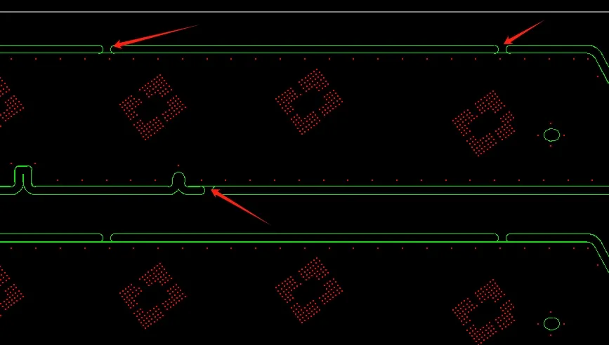
Figure 3: There are no stamp hole design
| Potential Failure Mode | Root Cause Linked to EQ | Likely Production Impact |
|---|---|---|
| Exposed copper at edge | Pad too close to outline | Scrap or rework after contour |
| Edge corrosion or shorts | Copper left after milling | Field reliability degradation |
| Micro-cracks from depanel | Solid ribs without stamp holes | Yield loss at final inspection |
| Marking interference | Unspecified production-number location | Cosmetic rejects or copper damage |
Table 2: maps each failure mode directly to the Engineering Question items
Failure Scenarios Prevented by Early Engineering Confirmation
Had the pad-to-outline issue been ignored, the contour routing step would have produced boards with ragged copper edges. These edges would fail visual inspection under IPC-A-600 criteria and could also cause intermittent shorts when the boards were later inserted into metal enclosures or stacked during shipping. In a worst realistic case the exposed copper would oxidize during storage, leading to poor solderability of nearby pads and elevated scrap rates at assembly.
Without stamp holes the depanelization process would have required breaking solid laminate bridges. On a long 582 mm panel the leverage amplifies stress, increasing the chance of copper lifting or solder-mask cracking near the break line. Such latent damage often escapes final electrical test yet appears later as open circuits after thermal cycling.
An unspecified production-marking location carries a quieter but equally practical risk. Operators might place the date code or serial number over a pad or too close to the edge, creating a new clearance violation that only becomes visible after silkscreen curing. The resulting boards would then require manual rework or complete scrap.
All three scenarios share a common origin: insufficient design-for-manufacturing detail at the outline interface. Preventing them required explicit customer confirmation before any tooling was released.
Preventive Actions Taken During the DFM Exchange
Our engineering team issued a focused Engineering Question that listed the three observations in priority order. The highest priority item requested confirmation on how to treat the pads that measured too close to the outline. Options typically include copper pull-back, pad relocation, or acceptance of a controlled exposure under specific conditions. The customer was asked to choose the approach that preserved electrical function while restoring a safe clearance.
For the missing stamp holes we recommended adding standard 0.8 mm or 1.0 mm diameter holes on each connection rib so that depanelization could occur cleanly along a perforated line. This change is low-cost and does not alter the final board outline.
Regarding the production number and date code, we asked the customer to designate a non-copper area or to allow the factory to place the marking in a standard location that maintains clearance to both copper and the board edge. Once the preferred location was confirmed, the fab drawing was updated and locked.
The customer reviewed the proposed adjustments, confirmed the preferred copper-pull-back strategy for the critical pads, accepted the addition of stamp holes, and supplied a clear coordinate for the production marking. With these answers in hand the CAM files were revised, the panelization verified, and the order released to production with a documented risk-mitigation trail.
| Action Item | Customer Decision | Manufacturing Benefit |
|---|---|---|
| Pad-to-outline clearance | Copper pull-back accepted | No copper exposure after contour |
| Stamp holes on ribs | Added as recommended | Clean depanelization, reduced stress |
| Production marking location | Coordinate supplied | No interference with copper or edge |
Table 3: records the closed-loop decisions that converted an uncertain design into a manufacturable one
Building Trust Through Early Clearance Verification
This case illustrates why Pad to Outline Clearance must be treated as a first-order DFM checkpoint rather than a secondary cosmetic item. On a 2-layer TG150 panel with no process edge, even a few tenths of a millimeter of insufficient clearance can produce exposed copper, edge defects, and later reliability problems. By raising the issue before tooling and obtaining customer confirmation, the engineering team eliminated the most probable sources of scrap and field returns.
Designers working with large customer-panelized boards are encouraged to include explicit edge-clearance rules in the fab drawing and to pre-place stamp holes on every connection rib. When production markings are required, a designated keep-out area prevents last-minute placement conflicts. These simple practices, verified during DFM review, convert potential manufacturing risks into controlled, documented decisions.
Proactive clearance verification remains one of the highest-leverage actions a DFM team can take to protect both yield and long-term board reliability.
FAQ
Q1: Why does Pad to Outline Clearance matter more on scored panels than on fully routed boards?
A1: Scoring leaves the final contour path almost identical to the design outline. Any copper that sits near that path is likely to be cut or left exposed. Fully routed boards with process edges allow the cutter to stay farther from copper features, reducing the same risk.
Q2: What realistic defects appear if copper is exposed after contour routing?
A2: Exposed copper can oxidize, create shorts against metal chassis, or act as a corrosion site under humidity. These defects often pass electrical test yet fail visual inspection or appear later in the field as intermittent failures.
Q3: How do missing stamp holes on connection ribs affect yield?
A3: Solid ribs require force to break. That force can lift copper or crack solder mask near the break line, producing scrap that only becomes visible after depanelization. Stamp holes convert the break into a controlled perforation and eliminate most of that stress.
Q4: Why must the location of production numbers and date codes be specified?
A4: Without a defined keep-out area the marking may land on copper pads or too close to the edge, creating new clearance violations or covering critical features. Specifying the location removes ambiguity and protects both electrical and cosmetic quality.
Q5: Can IPC standards help decide acceptable pad-to-edge distance?
A5: IPC-A-600 and IPC-6012 provide acceptability criteria for edge conditions and exposed copper. They do not prescribe an exact numerical clearance for every design, so manufacturers combine the standards with process capability data to set practical minimums during DFM review.
Q6: How can designers reduce the chance of similar Engineering Questions on future 2-layer panels?
A6: Include an explicit pad-to-outline clearance rule in the fab notes, pre-place stamp holes on every connection rib, and designate a non-copper zone for production markings. These three details, verified early, prevent the majority of edge-related DFM stops.