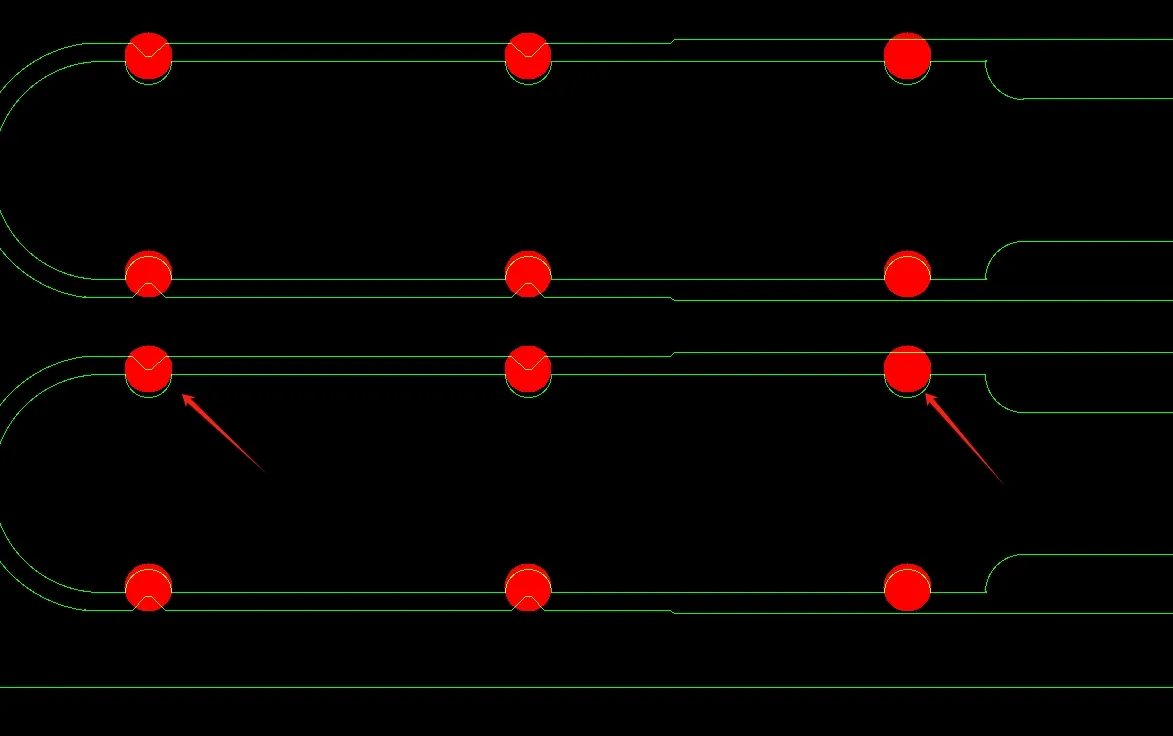
When a 2-layer FR-4 board measuring 323.77 × 379.03 mm arrived for production, the order parameters listed via tenting as the default treatment and lead-free HASL as the surface finish. Quantity stood at 6400 pieces in an 8×2 customer panel with V-groove separation. At first glance the data package appeared straightforward: 1.6 mm thickness, TG150 material, 1 oz / 2 oz copper, cool-white solder mask on both sides, and black silkscreen. Yet during CAM review the solder mask Gerber layers revealed a more complex picture. Some vias carried full openings, others carried reduced openings, while the system order explicitly called for tenting. This mismatch in PCB solder mask opening design immediately raised an Engineering Question. Production could not proceed until the design intent behind the mixed openings was clarified and reconciled with manufacturing capability.
Understanding the Original Design Intent Behind Mixed Via Treatments
The board ( #FR4-20260708-079 ) was a conventional 2-layer FR-4 design with a hole density of approximately 54 000 holes per square meter and a minimum finished hole size of 0.3 mm. Copper was specified at 1 oz inner and 2 oz outer, surface finish was lead-free HASL, and no impedance control or resin-plugged vias were required. The customer had chosen customer-panel format with V-groove separation and no process edge. Silkscreen was black on cool-white solder mask.
From the Gerber files it was evident that the designer had intentionally differentiated via treatments. A portion of the vias were drawn with full solder mask openings, another portion with smaller openings, while the order form itself defaulted to complete tenting. In parallel, certain SMT pads showed deliberate opening adjustments that the customer later described as a countermeasure against tombstoning, aiming to keep finished pad sizes consistent after HASL. The keep-out layer also contained rectangular features that overlapped active circuitry. Collectively these elements suggested a design that tried to balance electrical exposure, solderability, and PCB assembly yield, yet the documentation left the manufacturing interpretation ambiguous.
Initial CAM Observations on Solder Mask Opening Inconsistencies
Our CAM engineer first compared the solder mask Gerber layers against the order parameters. The system record stated ''via tenting,'' yet the artwork showed a mixture of open and partially open vias. Further measurement confirmed that the 0.3 mm vias carried openings whose size would normally trigger compensation under standard LPI processing. At the same time, selected SMT pads displayed enlarged or adjusted openings that appeared to equalize the final copper area after surface finish.
A rectangular feature on the keep-out layer was found to sit directly over circuit copper. Silkscreen characters near dense copper areas raised a secondary concern about legibility after HASL and mask curing. Finally, the V-groove panel arrangement lacked any indication of stamp holes at the connection points. Each of these observations was logged, but the dominant issue remained the conflict between the mixed solder mask openings in the Gerber data and the blanket tenting instruction on the order form.
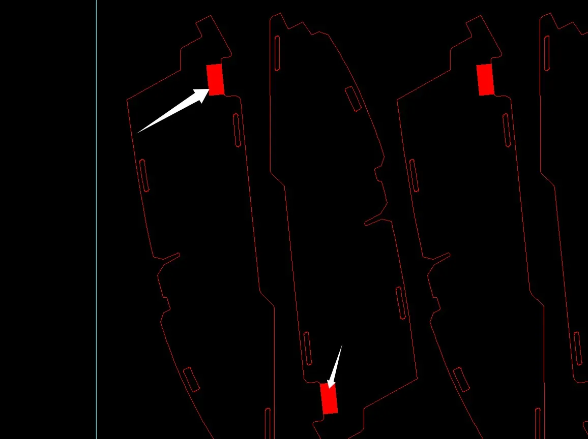
Figure 1: the rectangular design indicated by the arrow on the keepout layer overlaps with the copper layer
| Source | Via Treatment Stated | Observed in Gerber |
|---|---|---|
| Order parameters | Via tenting (full cover) | — |
| Solder mask Gerber | — | Mixed full openings + reduced openings |
| 0.3 mm vias | Tenting expected | Openings present; compensation question raised |
Conflict Analysis: PCB Solder Mask Opening Design Versus Order Specification
The primary design-to-manufacturing conflict centered on PCB solder mask opening design. The Gerber data contained intentional differentiation—some vias fully opened, others given only small openings—while the order form instructed complete tenting. If the factory simply followed the order and tented every via, the designer's selective exposure would be lost. Conversely, if the factory followed the Gerber openings without compensation, the 0.3 mm vias risked incomplete coverage or excess copper exposure after registration tolerance and LPI swell.
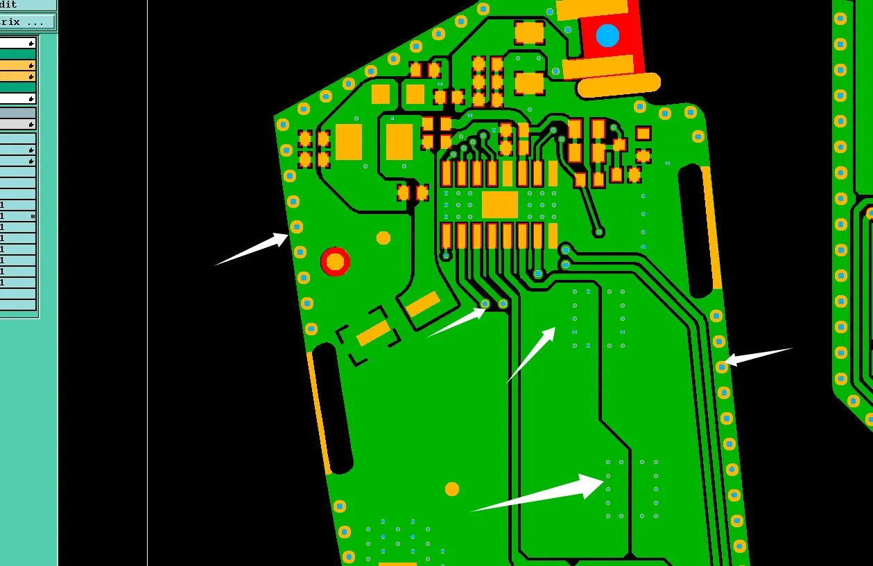
Figure 2: some vias are designed as open windows, while others are designed as small windows
Under typical liquid photoimageable solder mask processing, openings are expanded by a small amount (solder mask swell) to compensate for registration and develop variation. For vias at 0.3 mm, applying the normal compensation could enlarge the opening enough to leave annular copper exposed or, in the opposite direction, allow mask to encroach on the pad if no opening had been drawn. The customer's later comment that ''opening size must strictly follow the original manuscript'' and the suggestion that 0.3 mm vias should receive no compensation confirmed that the design intent was to preserve the exact opening geometry drawn in the Gerber files.
A secondary but related issue appeared on the SMT pads. Certain pads carried adjusted openings that the customer described as a countermeasure against tombstoning. The goal was to keep finished pad sizes consistent after HASL deposition so that component placement forces remained balanced. This practice is recognized in assembly literature, yet it further complicated the solder mask interpretation: the same layer that controlled via exposure also controlled pad openings intended to equalize copper area.
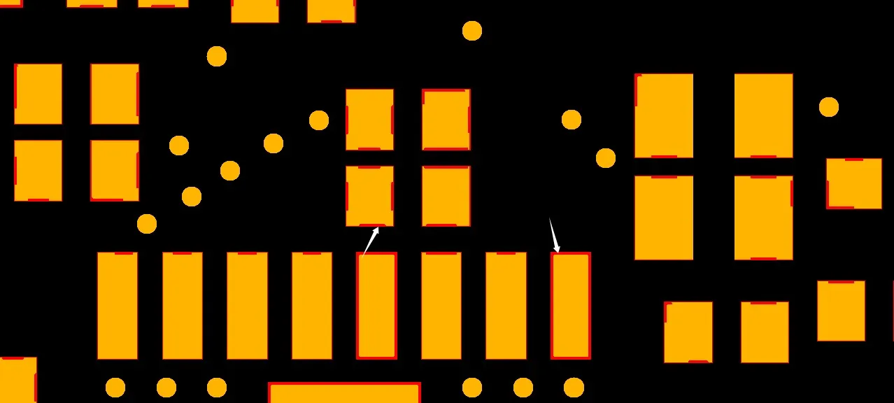
Figure 3: tombstone effect
From a manufacturing-risk standpoint, three realistic outcomes were possible if the conflict remained unresolved:
- Full tenting of every via would bury the intentional openings, potentially trapping flux or altering thermal paths during reflow.
- Strict adherence to the Gerber openings without compensation could produce undersized or oversized clearances once registration tolerance (±0.05–0.075 mm typical for LPI) was applied, risking solder bridges or exposed copper near the via barrels.
- Inconsistent pad openings could re-introduce the very tombstoning effect the designer had tried to prevent, lowering SMT yield on a high-volume 6400-piece run.
IPC-4761 Type I and Type II via protection guidelines acknowledge both tented and open vias as valid constructions, yet they presuppose that the choice is unambiguous in the fabrication data. Here the data were not unambiguous. The keep-out layer rectangle that overlapped active circuitry added another layer of interpretation risk: if the feature were treated as a mask keep-out it would create an unintended opening; if ignored it might leave mask over copper that the designer had intended to expose.
| Engineering Observation | Conflict Identified | Potential Manufacturing Outcome | Recommended Clarification |
|---|---|---|---|
| Mixed via openings in solder mask Gerber | Order specifies tenting | Loss of selective exposure or unintended copper exposure | Confirm which vias must remain open and whether compensation is allowed |
| 0.3 mm vias with openings | Standard swell vs. strict manuscript | Registration-induced clearance errors | Accept zero-compensation processing |
| Adjusted SMT pad openings | Tombstoning prevention intent | Uneven pad sizes after HASL | Preserve exact opening geometry |
Supporting Observations That Reinforced the Primary Concern
While the solder mask conflict remained the dominant issue, several secondary findings supported the need for full clarification before release. The rectangular feature drawn on the keep-out layer sat directly on circuit copper. Without customer instruction it was unclear whether the feature should be ignored or treated as an additional opening. Silkscreen characters located near dense copper zones were flagged because white or light-colored markings can become less distinct after HASL and mask curing; the customer was asked whether the finished appearance would still be acceptable. Finally, the 8×2 V-groove panel showed continuous copper bridges at the separation lines. Stamp holes were not present, raising the practical question of whether depaneling would be reliable without them.
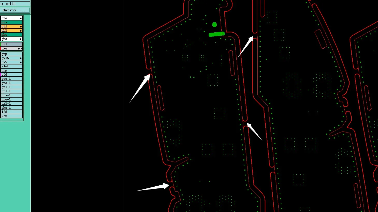
Figure 4: stamp holes were not present
Engineering Clarification and Final Manufacturing Resolution
An Engineering Question was issued that summarized the observed discrepancies and requested explicit confirmation on four points: (1) which vias were intended to remain open versus tented, (2) whether 0.3 mm vias should receive zero compensation so that the manuscript openings were preserved exactly, (3) whether the keep-out rectangle overlapping circuitry should be ignored, and (4) whether stamp holes were required at the V-groove connection points. The customer's responses were unambiguous.
The mixed openings were intentional. Vias drawn with openings were to remain open; vias without openings were to be tented. For the 0.3 mm vias the customer accepted the factory recommendation of zero compensation, thereby locking the opening size to the Gerber geometry. The keep-out rectangle was confirmed to be ignored. Stamp holes were not required. Silkscreen legibility after finishing was accepted as-is. The tombstoning-related pad openings were likewise to be processed exactly as drawn so that finished pad sizes remained balanced.
With these answers in hand the CAM data were revised. Solder mask openings for the designated vias were left at nominal size with no swell applied to the 0.3 mm population. Tenting was applied only where the Gerber contained no opening. The keep-out feature was removed from the manufacturing data set. Panelization proceeded with the original V-groove definition and no added stamp holes. Once the revised files were verified against the customer confirmations, the job was released to production under the original 3-day engineering lead time.
The resolution preserved the designer's selective via exposure, maintained the intended pad geometry for assembly yield, and eliminated any risk that automatic tenting or standard compensation would alter critical clearances. Because the clarification occurred before plating and mask application, no material or process scrap was incurred.
Key Design Lessons for 2-Layer FR4 PCB Designers
Several practical takeaways emerge from this review that can reduce similar Engineering Questions on future boards:
- When mixed via treatments (tented versus open) are required, state the rule explicitly in the fabrication notes rather than relying solely on Gerber artwork. A simple note such as ''vias with solder mask openings remain open; all others tented'' removes ambiguity.
- If zero compensation is mandatory for small vias, declare it in the notes. Standard LPI processes apply swell by default; an explicit instruction prevents unintended enlargement of 0.3 mm openings.
- Pad openings intended to equalize finished copper area after HASL should be accompanied by a short note explaining the tombstoning-prevention intent. This helps CAM engineers understand that the geometry is deliberate rather than a drafting error.
- Keep-out layer features that overlap active copper must be either clearly labeled or omitted. Ambiguous geometry on non-standard layers forces clarification cycles.
- For V-groove panels, indicate whether stamp holes are required at the break points. Their absence is acceptable on many designs, but the decision should be documented rather than left to factory interpretation.
- Silkscreen placed near dense copper or HASL areas benefits from a quick legibility check in the design phase. Light-colored ink on cool-white mask can lose contrast after thermal processing.
- Order-form defaults (such as ''via tenting'') should be reviewed against the actual Gerber content before submission. A mismatch between the form and the artwork is one of the most common triggers for Engineering Questions.
These practices do not add design time; they simply make the manufacturing interpretation of PCB solder mask opening design as clear as the electrical intent itself.
FAQ
Q1: Why did the factory question via openings that were already drawn in the Gerber files?
A1: The order form specified full via tenting while the Gerber layers showed selective openings. CAM review must reconcile the two sources; otherwise the factory cannot know which instruction takes precedence.
Q2: What is the risk of applying standard solder mask compensation to 0.3 mm vias that the designer wants left exact?
A2: Compensation (solder mask swell) enlarges the opening. On small vias this can leave annular copper exposed or allow mask to encroach on the pad once registration tolerance is added, altering the intended clearance.
Q3: How does partial solder mask opening design affect SMT assembly yield?
A3: When pad openings are adjusted to keep finished copper areas consistent after HASL, component placement forces remain balanced and tombstoning risk decreases. Changing those openings without confirmation can re-introduce the imbalance the designer tried to eliminate.
Q4: Should keep-out layer geometry that overlaps copper always be ignored?
A4: Not automatically. The feature may represent an intentional additional opening or a drafting remnant. Confirmation is required so that the manufacturing data set neither creates an unwanted opening nor covers copper the designer meant to expose.
Q5: Why is an explicit note about tented vias versus exposed vias preferable to relying only on Gerber artwork?
A5: Order forms and CAM software often default to a single treatment. A short fabrication note overrides the default and eliminates the need for an Engineering Question, accelerating release to production.
Q6: Can V-groove panels be released without stamp holes?
A6: Yes, provided the copper bridges are narrow enough for clean separation and the customer accepts the resulting edge condition. Documentation of the decision prevents later disputes about depaneling quality.