When a 2-layer FR-4 board measuring 14.33 × 23.11 mm arrives for a 50-piece order, the design files themselves may be electrically complete, yet the manufacturing package still requires targeted production engineering before the job can move to the shop floor. In this case the critical preparation centered on PCB stamp hole design. The customer data already showed connection positions intended for panel breakout, but no stamp holes were present. Additional questions arose about solder-mask treatment of the 0.6 mm holes and the currency of the production cycle marking. Resolving these items transformed a set of individual small boards into a production-ready panel that supports stable plating, clean depanelization, and reliable traceability.
Our CAM review treated the stamp-hole decision as the primary production-preparation activity. The remaining confirmations were handled as supporting steps that keep the overall manufacturing data package consistent and free of last-minute holds.
Small 2 Layer FR4 Board Project Overview and Panelization Needs
The order ( #FR4-20260510-065 ) defined a compact 2-layer construction: 1.6 mm FR-4, 1 oz outer copper, Immersion Gold at 1 µin, green solder mask, white silkscreen. Minimum hole size was 0.2 mm, minimum trace and space 4/4 mil, minimum annular ring 4 mil. Hole copper thickness was specified as 18 µm. Outline tolerance sat at ±0.2 mm, PTH hole tolerance ±0.075 mm, NPTH ±0.05 mm, with remaining features governed by IPC Class 2. UL marking was required. Electrical test would be performed by flying probe and shipment by DHL.
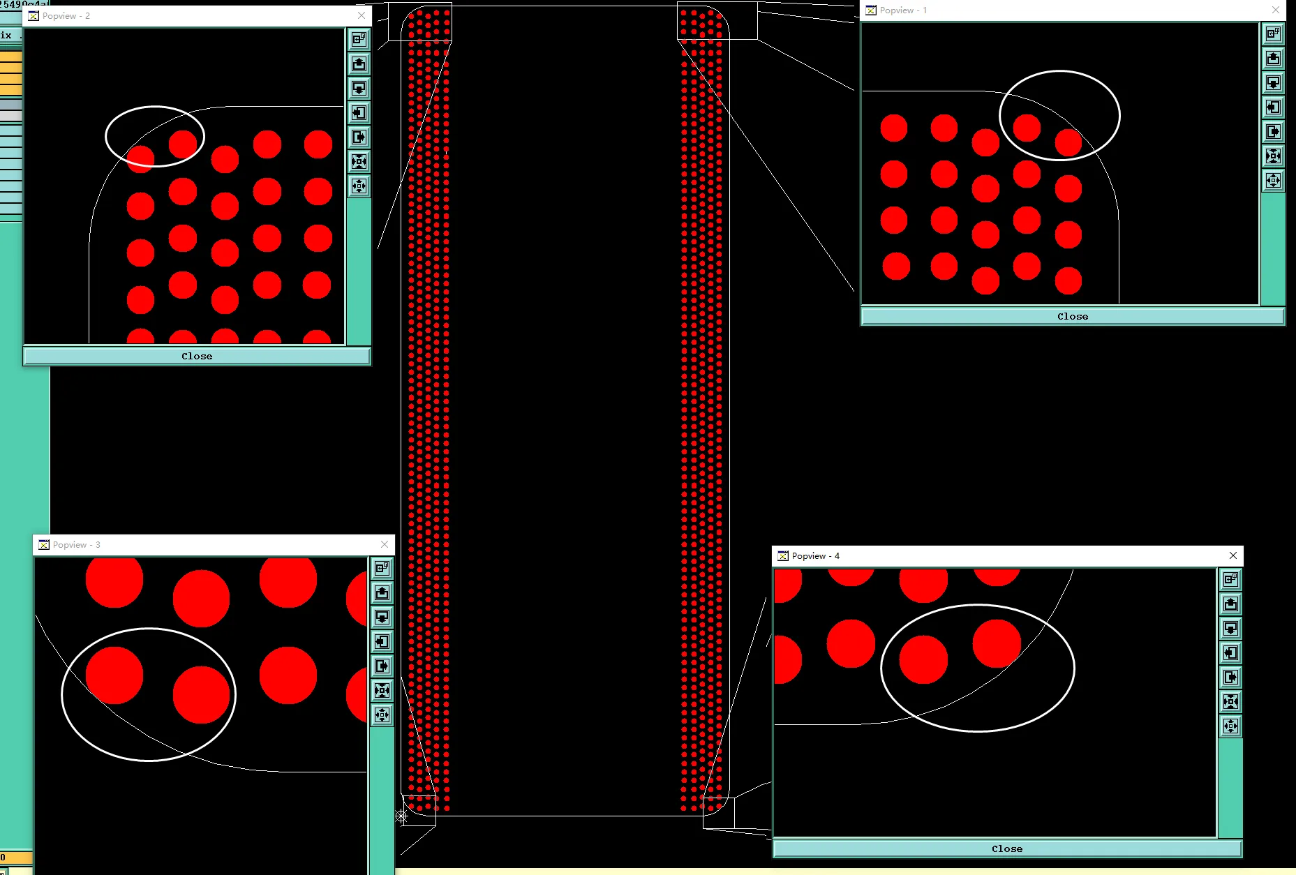
Because each finished unit is smaller than a typical process rail, single-board processing was impractical. Panelization was therefore mandatory for plating uniformity, solder-mask registration, and safe handling. The supplied data already indicated connection positions, yet those positions lacked stamp holes. Without them the only practical separation methods would be full outline routing or uncontrolled breaking—both of which increase cycle time or risk edge damage on boards of this size. The production package therefore needed a clear stamp-hole pattern before release.
Stamp Hole Placement Strategy for Clean Board Separation
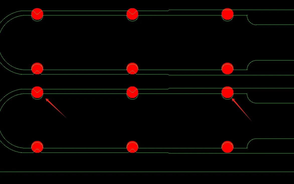
During the initial data review the CAM engineer observed multiple connection tabs whose geometry was suitable for breakout, yet no stamp holes (mouse bites) appeared at those locations. Leaving solid tabs would force either a continuous routing cut around every board or manual breaking after final test. Continuous routing lengthens CNC time and generates more debris; manual breaking on a 14 mm × 23 mm board risks fracture or irregular edges that fail visual inspection under IPC-A-600 criteria.
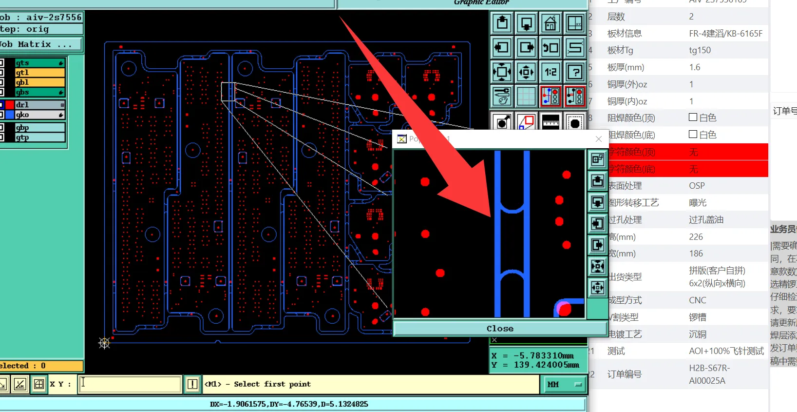
Figure 1: the data already indicated connection positions, yet those positions lacked stamp holes
The engineering recommendation was therefore to add a standard stamp-hole array across each connection tab. Typical practice places three to five holes of 0.8–1.0 mm diameter on a short pitch so that the remaining web thickness maintains panel rigidity through wet processes while remaining weak enough for clean separation. The hole centers were positioned relative to the final board outline so that the break line stays inside the ±0.2 mm outline tolerance. Clearance to nearby copper features was verified to avoid any risk of exposed copper after breakout.
Customer confirmation of the stamp-hole addition locked the panel geometry. Once approved, the drill file and routing program could be updated in a single pass, eliminating a potential source of first-article delay. The same stamp-hole pattern also simplified process-rail design: the outer rails could now be sized for standard tooling pins and fiducials without interfering with the break points.
| Option | Advantage | Risk if Incorrect |
|---|---|---|
| Add Standard Stamp Holes | Clean breakout, maintains panel strength | Minimal when properly sized |
| Leave Solid Tabs | No extra drill time | Warpage, irregular edges, higher scrap |
| Full Outline Routing | Complete separation | Longer CNC time, more debris |
Table 1: Stamp Hole Design Options and Impacts
Solder Mask Treatment Decision for 0.6 mm Holes
A second production-preparation item concerned the 0.6 mm holes. The supplied solder mask data showed openings over these holes, yet the engineering question asked whether the openings should be retained or deleted so that the holes would be tented (covered with solder mask). On boards of this density a tented via reduces the risk of solder wicking during assembly and protects the hole wall from contamination. Retaining the opening, by contrast, leaves the hole available for test or secondary processes but increases the chance of mask residue inside the barrel if the opening is marginal relative to the hole diameter.
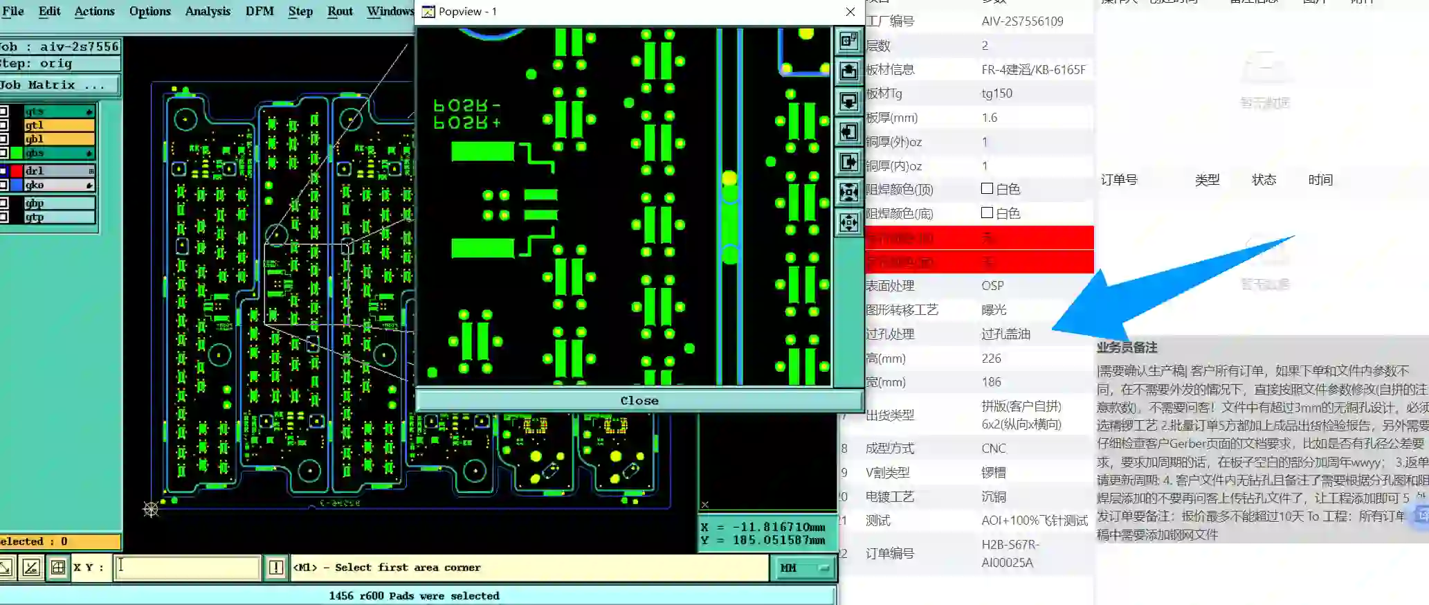
Figure 2: the supplied solder-mask data showed openings over these holes
Because the minimum annular ring is only 4 mil and the hole size is close to the lower practical limit for reliable tenting, the decision required explicit confirmation. The production package could not proceed with an ambiguous solder-mask layer. Once the customer elected the preferred treatment—either open window or full tenting—the CAM data were adjusted accordingly and the mask plot regenerated. This single clarification prevented a potential mismatch between the solder-mask artwork and the intended manufacturing outcome.
Updating the Production Cycle Marking
The third item concerned the production cycle marking. The data contained an existing period or date-code legend; the engineering question asked whether the indicated location should be updated to the latest cycle code. Traceability markings are placed on the process rail rather than on the functional board area so that the limited real estate of the 14 mm × 23 mm units remains fully usable. Updating the cycle code ensures that every panel leaving the line carries the correct manufacturing period, supporting both internal lot tracking and any customer requirement for date-code visibility after depanelization.
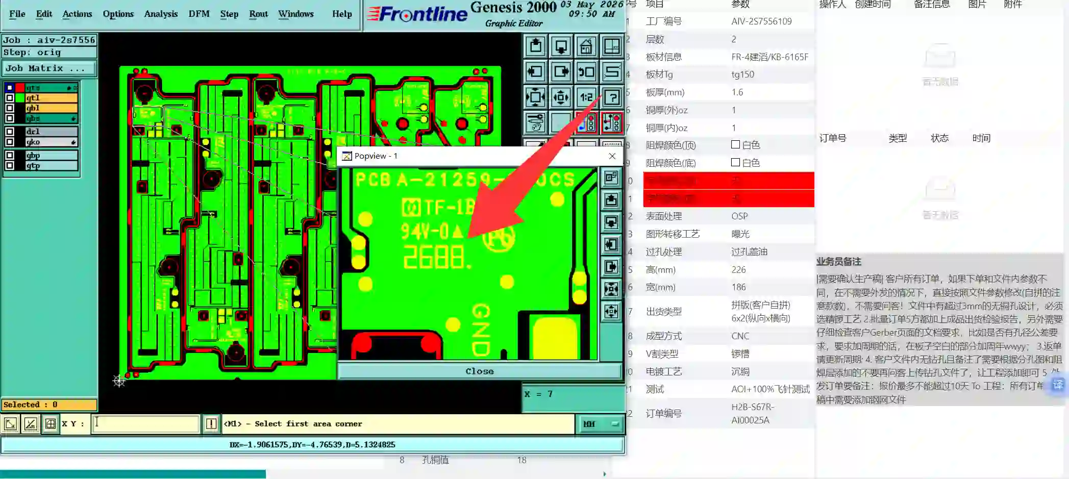
Figure 3: updating the cycle code
Because UL marking was also required, the cycle-code field was coordinated with the UL legend location on the same process rail. This arrangement keeps both identifiers readable after breakout while preserving the functional surface of each board. Confirmation of the updated cycle code completed the set of production markings and allowed the panel drawing to be frozen.
Panel Layout Optimization with Stamp Holes for Process Efficiency
With the stamp-hole pattern, solder-mask treatment, and cycle-code update confirmed, the manufacturing package could be optimized for throughput. The board size permitted a high-density array while still leaving adequate process-rail width for standard 3.175 mm tooling pins and fiducials. The stamp holes were coordinated with the final outline routing path so that the CNC program could complete both the board perimeter and any remaining large openings in a single setup, reducing tool changes and registration risk.
Process rails were designed to accept the factory's standard plating and solder-mask fixtures. This eliminated the need for special tooling and allowed the panel to move through the line on the same schedule as other 2-layer jobs of similar size. The UL mark and updated cycle code were placed on the rail in locations that remain visible after depanelization, satisfying both regulatory and traceability requirements without consuming functional board area.
The resulting panel drawing, updated drill file, solder-mask plot, and routing program formed a complete, self-consistent manufacturing package. Once customer confirmation of the three engineering questions was received, the job could be released without further CAM holds.
Production Readiness Checklist After Stamp Hole Confirmation
Before the manufacturing files were released, the following items were verified against the resolved engineering questions:
- Stamp holes added at every existing connection position to enable controlled depanelization.
- Stamp-hole geometry positioned to maintain ±0.2 mm board-outline tolerance after breakout.
- Solder-mask treatment of 0.6 mm holes confirmed (open window or tented) and mask plot updated.
- Production cycle marking updated to the latest period and coordinated with UL legend placement.
- Process rails sized for standard tooling pins and fiducials.
- Panel drawing, drill file, and routing program cross-checked against the original customer data.
- Final manufacturing package released for production scheduling.
Final Production Outcome with Optimized Stamp Hole Design
The engineering preparation converted a set of individual 14.33 × 23.11 mm boards into a robust, high-utilization panel ready for immediate fabrication. The addition of stamp holes delivered clean, low-stress depanelization while preserving panel strength through plating and mask processes. Clarification of the 0.6 mm hole solder-mask treatment removed any ambiguity in the mask artwork. Updating the cycle code ensured correct lot traceability without consuming functional board area. Together these steps eliminated the classic sources of first-article delay that often accompany very small boards—uncertain separation methods, conflicting mask instructions, and outdated production markings.
The manufacturing package that left the CAM department therefore required no further engineering clarification. Production could proceed directly from the released files, achieving the intended combination of process efficiency, dimensional consistency, and on-time delivery for the 50-piece order.
FAQ
Q1: Why are stamp holes required when connection tabs already exist in the design data?
A1: Solid connection tabs leave a continuous web of laminate that is difficult to break cleanly. Stamp holes create controlled weak points so that individual boards can be separated without stressing the small units or leaving irregular edges that fail visual inspection.
Q2: What is the practical difference between an open solder-mask window and tenting on a 0.6 mm hole?
A2: An open window leaves the hole available for test or secondary processes but increases the chance of mask residue inside the barrel. Tenting covers the hole with solder mask, reducing solder wicking during assembly and protecting the hole wall from contamination. The choice must be confirmed before the mask plot is released.
Q3: Can a PCB factory produce boards of this size without panelization?
A3: Single-board processing is theoretically possible but inefficient. Handling, plating uniformity, and solder-mask registration all suffer when the workpiece is smaller than typical process fixtures. Panelization remains the practical method for maintaining quality and throughput.
Q4: Why must the production cycle marking be confirmed even when a date-code legend already exists?
A4: The existing legend may reflect an earlier manufacturing period. Updating it to the latest cycle code ensures correct lot traceability and keeps the marking consistent with the actual production date of the panel.
Q5: How does proper PCB stamp hole design improve overall manufacturing efficiency?
A5: A well-designed stamp-hole pattern allows the panel to remain rigid through wet processes yet separate cleanly after test. This reduces CNC routing time, minimizes edge defects, and supports higher panel utilization—directly shortening cycle time and improving yield on small-board orders.
Q6: What happens if stamp holes are omitted from a panel that contains only solid connection tabs?
A6: Separation then relies on either full outline routing (adding cycle time and debris) or manual breaking (risking board damage and irregular edges). Both alternatives increase cost and quality risk compared with a properly designed stamp-hole pattern.
```