PCIe SSDs have become the backbone of high-performance storage in consumer, enterprise, and automotive systems. From a PCB engineering viewpoint, these drives impose demanding requirements on high-speed differential routing, power delivery networks, thermal dissipation, signal integrity, and long-term reliability. Whether implementing consumer PCIe 4.0 modules or rugged automotive CXL solutions, PCB design and manufacturing choices directly determine achievable bandwidth, endurance, and operational stability.
3D NAND Layer Scaling and PCB Thermal-Mechanical Challenges
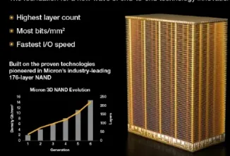
The race toward 300-layer 3D NAND dramatically increases storage density while introducing new PCB-level constraints. Stacking hundreds of layers requires precise control of warpage, thermal expansion, and heat dissipation within the package and on the host board. PCB designers must select high-Tg laminates, optimize copper thickness for heat spreading, and incorporate thermal vias or metal-core substrates beneath the SSD controller and NAND packages. As layer counts rise, localized heating from program/erase operations intensifies, necessitating careful placement of heat sinks, thermal interface materials, and airflow considerations in the overall system enclosure. Manufacturing processes such as lamination and via filling must accommodate the finer features and higher aspect ratios demanded by next-generation NAND packages.
PCIe 4.0 and Emerging Interfaces: Routing and Signal Integrity on SSD PCBs
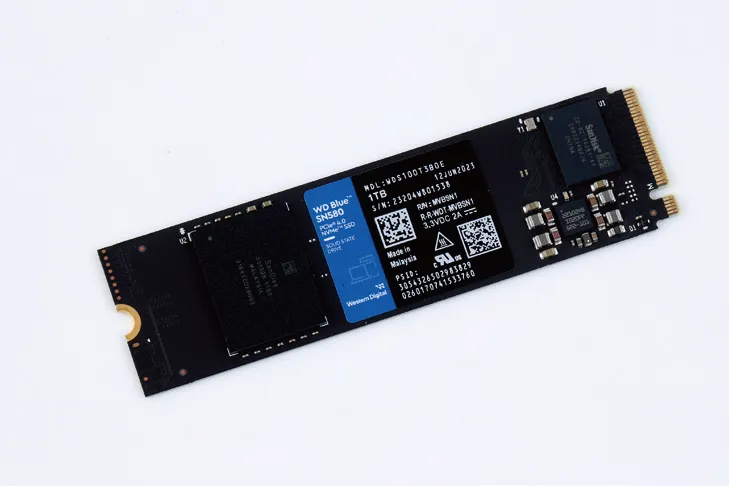
PCIe 4.0 SSDs, exemplified by models such as the WD Blue SN580, deliver sequential speeds approaching 5,000 MB/s through x4 lanes at 16 GT/s. Achieving these rates on the module PCB requires controlled-impedance differential pairs, minimal via stubs, and precise length matching across all high-speed traces. The GALAX Star Yao 7000 Plus and similar high-performance drives further highlight the need for low-loss dielectrics and optimized stack-ups to support PCIe 5.0 and beyond. On the host motherboard, PCIe root-complex routing must maintain signal integrity over longer distances while managing crosstalk and return-path discontinuities. Back-drilling, via-in-pad, and HDI techniques become essential to support the dense pin counts of modern SSD controllers.
QLC NAND Endurance and PCB Power Delivery Optimization
QLC NAND offers compelling cost-per-bit advantages but trades off endurance and write performance compared with TLC. When evaluating whether QLC all-flash arrays can replace hybrid storage configurations, PCB engineers must address the higher program/erase cycle demands and the resulting power consumption spikes. Robust power delivery networks with ample decoupling capacitance, low-ESR capacitors, and properly sized power planes are critical to maintain stable voltage during intensive write workloads. Wear-leveling algorithms at the controller level are supported by clean, low-noise power rails on the PCB, while thermal management prevents temperature-induced endurance degradation. Hybrid designs that combine QLC with faster SLC or TLC caches require careful partitioning of power domains and thermal zones on the same board.
Automotive CXL and PCIe SSD Solutions: Reliability and Harsh-Environment PCB Design
Automotive-grade CXL and PCIe SSDs must operate reliably across wide temperature ranges, high vibration, and strict functional-safety standards. PCB designs incorporate AEC-Q200 qualified components, extended-temperature laminates, and conformal coatings. Redundant power paths, vibration-resistant via structures, and enhanced EMI shielding protect against the harsh electrical and mechanical environment of vehicles. CXL interfaces add cache-coherent memory semantics that demand even tighter timing margins and lower latency interconnects, pushing PCB technology toward finer features and advanced materials. Early stack-up definition and thermal simulation help ensure these storage modules meet ISO 26262 requirements while delivering the bandwidth needed for real-time data logging and AI inference in autonomous systems.
Consumer SSD Module PCB Layout Best Practices
Reviews of drives such as the WD Blue SN580 and GALAX Star Yao 7000 Plus reveal common PCB optimization patterns. Compact M.2 or U.2 form factors favor HDI routing to accommodate dense NAND and DRAM packages. Strategic placement of the SSD controller, DRAM cache, and NAND arrays minimizes trace lengths for high-speed signals while allowing adequate copper area for power and heat spreading. Proper grounding schemes, split power planes, and EMI suppression components ensure compliance with regulatory limits and stable operation under varying system loads. These layout techniques directly influence sustained performance, power efficiency, and long-term reliability reported in real-world testing.
Future Trends: 300+ Layer NAND and Next-Generation Storage PCB Manufacturing
Continued scaling to 300 and more NAND layers, combined with PCIe 6.0/7.0 and CXL 3.0 adoption, will further intensify demands on PCB technology. Low-loss materials, embedded capacitors, and 3D packaging-compatible stack-ups will become standard. Automotive and edge AI applications will drive demand for boards that balance extreme density with automotive-grade durability. Close collaboration between SSD architects and automotive PCB manufacturers during the design phase enables optimized material selection, via technology, and surface finishes that support both performance targets and production yields.
Conclusion
PCIe SSD performance, endurance, and reliability ultimately depend on PCB-level engineering decisions that address high-speed signal integrity, thermal management, power delivery, and harsh-environment robustness. As 3D NAND layer counts climb and automotive CXL deployments accelerate, early partnership between storage system designers and specialized PCB manufacturers is essential to achieve cost-effective, high-yield solutions that meet evolving bandwidth and durability requirements. Aivon’s expertise in advanced multilayer, HDI, and automotive-qualified PCB fabrication provides the technical foundation needed to realize the full potential of next-generation SSD architectures across consumer, enterprise, and automotive markets.