Vision sensors, millimeter-wave (mmWave) radar, and LiDAR form the core perception suite for autonomous driving and advanced driver-assistance systems (ADAS). In PCB manufacturing and design, integrating these heterogeneous sensors requires optimized layouts, high-speed signal integrity, RF performance, thermal management, EMI/EMC compliance, and automotive-grade reliability. Multi-sensor fusion, SLAM algorithms, and real-time perception processing further demand advanced PCB stack-ups, HDI technology, and robust power delivery to achieve the safety, accuracy, and long-term durability required for production vehicles.
Vision Sensors on PCBs: Design Considerations and Performance Optimization
Vision sensors (cameras and image sensors) capture rich semantic information but are sensitive to lighting, weather, and obstructions.
On the PCB, successful integration involves:
- Precise sensor placement with controlled-impedance MIPI CSI-2 or parallel interfaces to preserve high-resolution image data.
- Dedicated low-noise analog and digital power domains with extensive decoupling to minimize image artifacts.
- Thermal vias, copper pours, and heatsink mounting for image signal processors (ISPs) and high-resolution sensors that generate significant heat during continuous operation.
- EMI shielding and ground plane strategies to prevent interference from nearby radar or power electronics.
Automotive PCBs must support AEC-Q100 qualified components, vibration-resistant mounting, and conformal coating while maintaining optical alignment tolerances during thermal cycling.
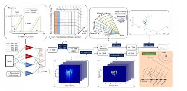
mmWave Radar PCB Integration and 4D Radar SLAM Approaches
mmWave radar excels in all-weather, long-range detection and velocity measurement. Modern 4D imaging radar adds elevation information, increasing channel count and data bandwidth. PCB design priorities include:
- RF-optimized stack-ups with low-loss materials (Rogers, PTFE, or hybrid constructions) for 76–81 GHz operation.
- Controlled-impedance microstrip or stripline routing for antenna feeds and high-speed digital outputs.
- Dense via stitching and power planes to support high-channel-count MIMO arrays.
- Thermal management for high-power transmitter/receiver modules.
4D radar SLAM implementations on PCBs require high-performance processors, large memory bandwidth, and low-latency interconnects. Designers often use HDI with micro-vias and embedded components to fit complex radar modules into compact automotive ECUs while maintaining signal integrity across temperature extremes.
LiDAR PCB Design: Core Parameters, Classification, and Integration Challenges
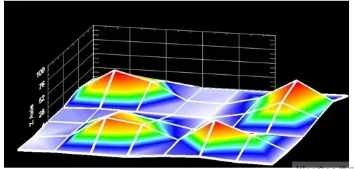
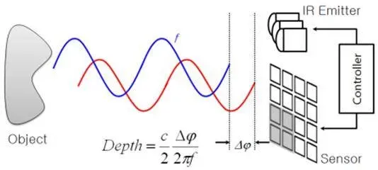
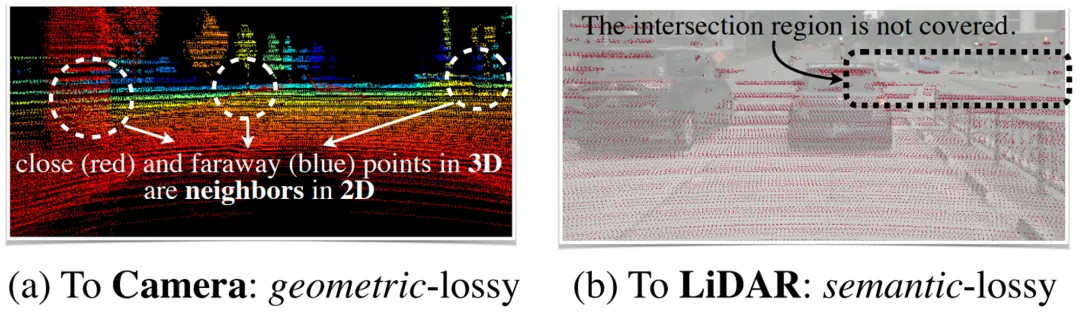
LiDAR provides high-resolution 3D point clouds essential for precise mapping and obstacle detection. Automotive LiDAR systems vary by scanning method (mechanical, MEMS, flash, or solid-state) and wavelength. PCB-level considerations include:
- High-speed data interfaces (Ethernet, PCIe, or proprietary) with strict timing and impedance control.
- Robust power delivery for laser drivers and photodetector arrays, often requiring heavy copper layers and multiple thermal vias.
- Mechanical stability and vibration damping for scanning mechanisms or MEMS mirrors.
- Optical window alignment features and EMI shielding to protect sensitive receiver electronics.
Trade-offs between LiDAR and vision (range vs. cost, resolution vs. weather resilience) directly influence PCB architecture—LiDAR modules typically need more complex thermal and RF isolation than camera modules.
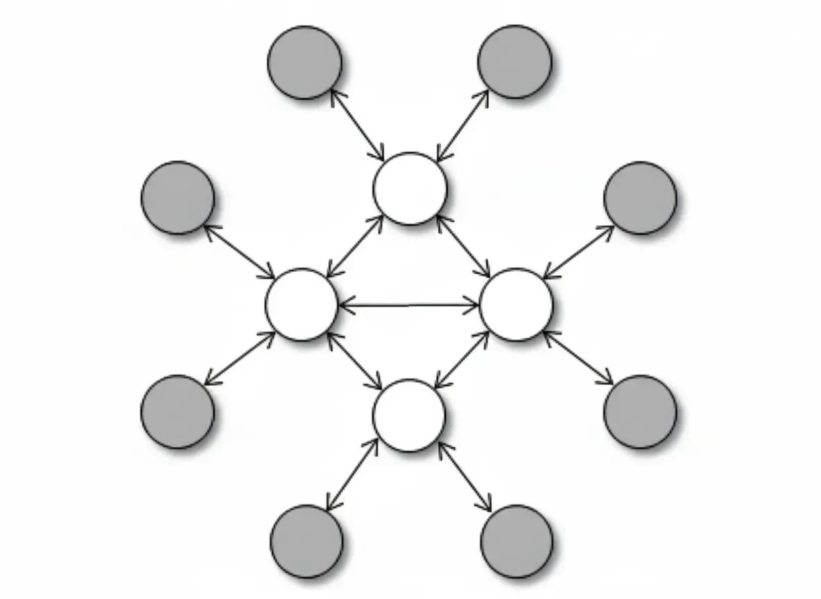
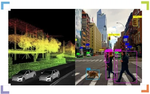
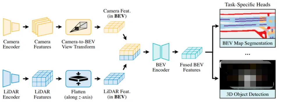
Multi-Sensor Fusion and Unified BEV Representation on PCBs
Effective autonomous perception relies on fusing camera, radar, and LiDAR data into a unified bird's-eye-view (BEV) representation.
This demands:
- High-bandwidth interconnects and low-latency buses between sensor modules and central processing units.
- Powerful edge AI processors with adequate thermal dissipation and memory support on the PCB.
- Synchronized timing across sensors using precise clock distribution networks.
- Redundant power paths and functional safety features (ISO 26262) to ensure continued operation if one sensor fails.
PCB designers must balance power consumption, heat generation, and signal integrity while fitting multiple high-performance modules into space-constrained automotive enclosures.
SLAM Implementation and Future Trends on Automotive PCBs
Simultaneous Localization and Mapping (SLAM) algorithms run on the vehicle's computing platform, requiring PCBs with high-performance SoCs, large DRAM/Flash capacity, and efficient cooling. Emerging approaches such as 4D radar SLAM and neural radiance fields (NeRF) for dynamic scene reconstruction increase computational load, pushing PCB technology toward:
- Advanced HDI and any-layer via structures.
- Embedded die and heterogeneous integration.
- High-Tg, low-loss materials for sustained high-frequency operation.
- Rigorous reliability testing including thermal shock, vibration, and power cycling.
Future trends point toward tighter sensor fusion, AI-accelerated perception, and cost-optimized solid-state LiDAR—all of which rely on increasingly sophisticated PCB manufacturing capabilities.
Conclusion
Vision, mmWave radar, and LiDAR sensors deliver the perception foundation for autonomous vehicles only when seamlessly integrated through optimized PCB design and manufacturing. By addressing RF performance, high-speed signaling, thermal management, multi-sensor synchronization, and automotive-grade reliability from the outset, engineers achieve superior detection accuracy, robust all-weather operation, and the functional safety required for production deployment. As multi-sensor fusion and SLAM algorithms grow more complex, specialized PCB solutions remain the critical enabler for scalable, high-performance autonomous driving systems. Aivon's advanced manufacturing capabilities—including RF materials, HDI, heavy copper, and high-reliability automotive processes—support the demanding requirements of next-generation perception platforms.