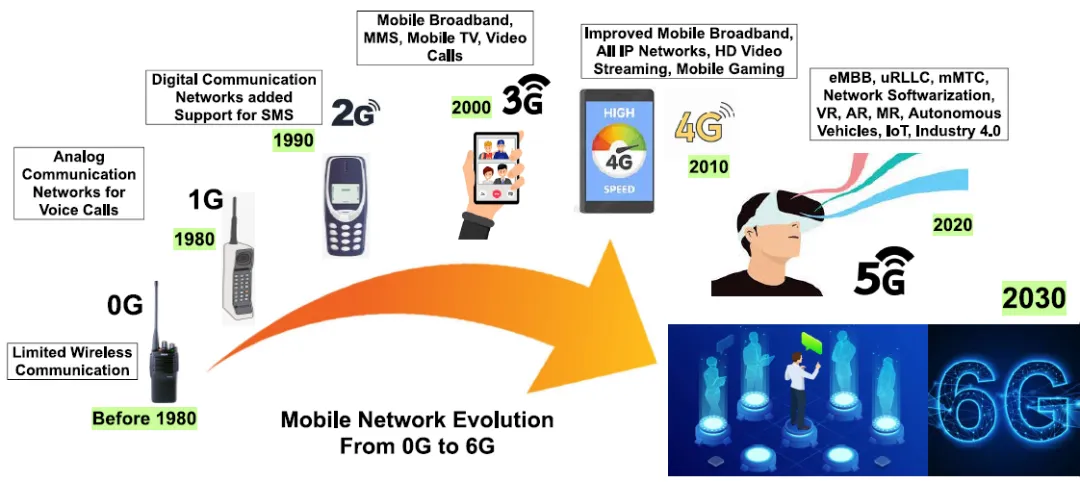
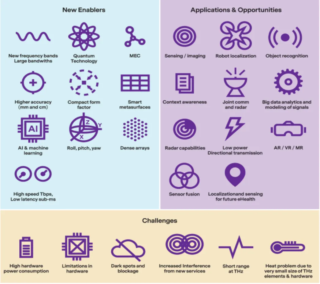
6G is poised to push wireless communications far beyond 5G, targeting terahertz frequencies, peak data rates exceeding 1 Tbps, sub-millisecond latency, and native AI integration. These ambitious goals create unprecedented demands on printed circuit board (PCB) technology. At Aivon, we are actively developing the advanced PCB solutions required for 6G infrastructure and devices, focusing on ultra-low-loss materials, 3D heterogeneous integration, high-density interconnects, and superior thermal/signal integrity to overcome the technical limits of next-generation wireless systems.
Key Driving Trends and Use Cases Reshaping PCB Requirements
6G targets transformative applications including holographic communications, digital twins, immersive XR, autonomous systems, and integrated sensing and communication (ISAC). These use cases demand extreme bandwidth, massive connectivity, and deterministic performance.
From a PCB engineering viewpoint, this translates to:
- Terahertz Frequency Support: Frequencies from 100 GHz to 1 THz require ultra-low Dk/Df materials and minimized transmission line lengths to control dielectric and conductor losses.
- Ultra-High Data Throughput: Routing for 100G+ SerDes interfaces with stringent impedance control (±5%) and back-drilling to reduce stub effects.
- Sensing Integration: Joint communication and radar-like sensing capabilities necessitate precise antenna array layouts and synchronized multi-channel RF paths on the same board.
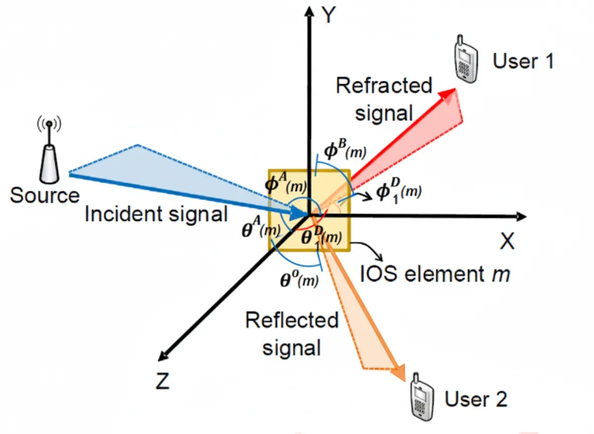
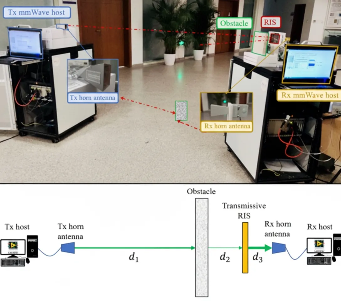
Pushing Technical Limits: Massive MIMO and Transmissive RIS
Massive MIMO in 6G will scale to thousands of antenna elements, while Reconfigurable Intelligent Surfaces (RIS), particularly transmissive RIS, will intelligently shape wireless propagation environments.
PCB-level challenges and solutions include:
- Extremely Dense Antenna Arrays: HDI and microvia technology with stacked vias to support massive element counts in compact form factors while maintaining phase coherence.
- Beamforming Complexity: Low-jitter clock distribution networks and synchronized power delivery across hundreds of RF chains.
- Transmissive RIS Implementation: PCBs designed as intelligent surfaces with embedded tunable elements, requiring multilayer constructions with precise via shielding and minimal insertion loss for efficient signal redirection.
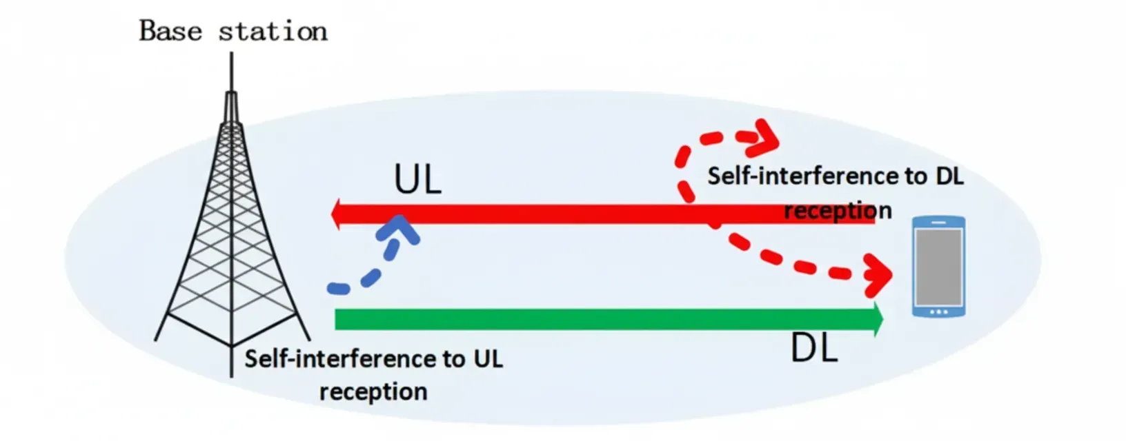
- Interference Management: Advanced ground plane designs, via fencing, and compartmentalized shielding to handle extreme spatial multiplexing without self-interference.
Native AI Architecture and On-Board Processing Demands
6G envisions AI-native networks where intelligence is embedded across devices, edges, and core. This requires significant on-board computational capability.
PCB design adaptations include:
- Heterogeneous Integration: Close integration of AI accelerators, baseband processors, and RF components through 2.5D/3D packaging.
- High-Speed Memory Interfaces: Controlled impedance routing for GDDR/HBM memory with minimal crosstalk in dense digital sections.
- Power Efficiency Optimization: Multi-domain PDNs with dynamic voltage scaling and extensive decoupling to support AI workloads without excessive heat or voltage droops.
- Thermal Management: Embedded copper coins, metal-core substrates, or advanced microvia thermal arrays to dissipate heat from high-performance AI engines operating alongside sensitive RF circuits.
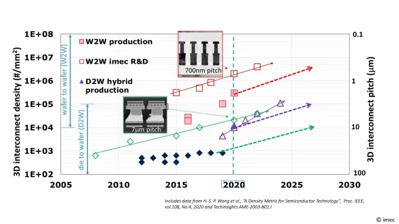
3D and Heterogeneous Integration for 6G Systems
Traditional 2D PCBs will be insufficient for 6G density and performance targets. 3D heterogeneous integration becomes essential.
Key manufacturing considerations:
- 3D Stacking Technologies: Through-silicon vias (TSV) interposers, package-on-package (PoP), and embedded component designs that combine logic, memory, and RF dies in compact vertical structures.
- Hybrid Material Stack-Ups: Combining low-loss THz-capable laminates with high-Tg cores and specialized dielectric layers for mixed-signal performance.
- Miniaturization and Reliability: Laser drilling, sequential lamination, and advanced plating processes to achieve high aspect ratio microvias while ensuring long-term reliability under thermal and mechanical stress.
- Signal Integrity in 3D: Careful modeling of vertical interconnects to prevent reflections and mode conversion at ultra-high data rates.
Addressing 6G Technical Limits Through Advanced PCB Engineering
6G pushes limits in spectrum, energy efficiency, and complexity. PCB solutions directly mitigate these:
- Material Innovation: Development of novel low-loss, low-Dk substrates capable of THz operation with stable electrical properties across temperature variations.
- Power and Thermal Co-Design: Heavy copper PCBs combined with liquid cooling interfaces or advanced thermal interface materials for base stations and high-end devices.
- EMI/EMC and Isolation: Comprehensive via stitching, shielding cans, and ground plane optimization to manage extreme bandwidth and massive connectivity without compromising performance.
- Testing and Validation: Rigorous RF characterization, thermal cycling, and high-speed signal integrity testing throughout the manufacturing process.
Deployment Timeline: From 5G-Advanced to 6G Readiness
While 5G-Advanced (5.5G) continues to roll out, 6G commercialization is expected in the early 2030s. Early research prototypes and testbeds already require cutting-edge PCBs to validate concepts in real environments.
Aivon supports this transition by providing:
- Scalable manufacturing from research prototypes to potential volume production.
- Collaborative design services for 6G-specific challenges in Massive MIMO, RIS, and ISAC.
- Future-proof material and process capabilities that bridge current 5G requirements with emerging 6G demands.
The journey to 6G represents a fundamental evolution in wireless technology that will be enabled - or constrained - by PCB design and manufacturing excellence. Higher frequencies, native AI, 3D integration, and intelligent surfaces all depend on superior signal integrity, thermal performance, and interconnect density.
Aivon delivers the advanced PCB engineering expertise necessary to turn 6G visions into reliable, high-performance reality across telecom infrastructure, industrial applications, and next-generation consumer electronics.