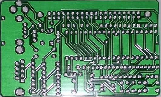
FPC Gerber outline mismatch between layers is a frequent cause of production delays and scrap. When the GM layer and GM1 layer don’t align properly, laser routing, coverlay cutting, or final profiling goes wrong. Understanding flex PCB GM layer issues helps designers submit clean files the first time.
Common Differences Between GM and GM1 Layers
Many designers assume GM and GM1 are identical. In reality, they often differ. One layer may contain the final routed outline while the other includes panel tabs, mouse bites, or fiducials for processing. These mismatches create confusion during CAM preparation.
Common issues include offset outlines, missing arcs or complex contours on one layer, or different handling of internal cutouts. Sometimes one file has the true product outline while the other still shows the array border.

Typical Root Causes in Layout Software
Outline layers get out of sync when designers edit one copy but forget to update the other. Copy-paste errors, different keep-out or dimension layers being exported, or last-minute changes to panelization all contribute to FPC Gerber outline mismatch.
In complex rigid-flex designs the problem appears more often because of multiple profile definitions across zones.
How Factories Decide Which Layer to Use
Most flex manufacturers default to the GM1 layer for final routing because it is conventionally treated as the primary outline in many CAD tools. However, experienced CAM engineers will compare both layers and choose the most complete and accurate one.
If the layers conflict significantly, production stops for clarification. This back-and-forth costs time and risks the manufacturer making an assumption that doesn’t match your design intent.

Consequences of Layer Mismatch During Production
Wrong outline selection can result in parts cut too small or too large, damaged traces near the edge, or incorrect tab placement that affects depanelization. In severe cases, entire panels are scrapped.
Preventing Flex PCB GM Layer Issues at Design Stage
The best solution is to maintain strict consistency between outline layers from the beginning. Use a single source of truth for the board outline in your CAD tool and generate both GM and GM1 from it.
Before exporting Gerbers, run a layer comparison check. Overlay GM and GM1 in a viewer and look for any differences in contours, cutouts, or dimensions.
Best Practices for Clean Gerber Output
- Define the final outline on one dedicated layer and copy it accurately.
- Avoid manual editing of exported Gerbers.
- Include clear fabrication notes specifying which layer is the authoritative outline.
- Use your CAD tool's built-in outline verification features.

Additional Checks Before Sending Files
Review all mechanical layers, drill drawings, and panelization borders. Make sure fiducials and tooling holes align with the chosen outline. For arrayed panels, confirm that breakaway tabs and mouse bites are correctly placed on the working outline layer.
A few minutes of careful verification during design prevents hours of engineering questions and potential re-taping later.
Key Lessons for Avoiding FPC Gerber Outline Mismatch
Treating GM and GM1 layers with equal importance and keeping them synchronized eliminates most flex PCB GM layer issues. Consistent outline definition is a small discipline that delivers big improvements in manufacturing efficiency and product quality.
Make outline layer verification a standard step in your release checklist. Your CAM team will notice the difference immediately, and your boards will come back right the first time.