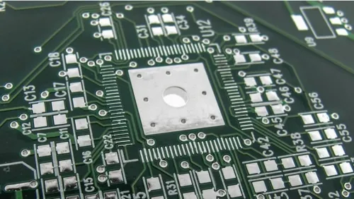
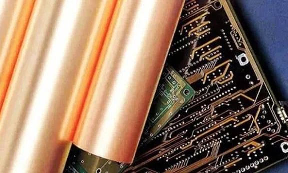
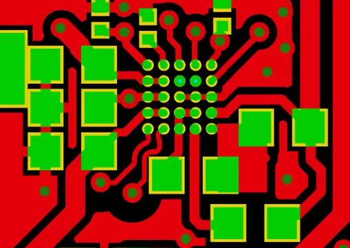
In HDI production we treat thermal relief as a controlled thermal break between a pad or via and the surrounding plane copper. CAM engineers flag any solid connection to a large copper pour on layers that will see reflow or selective soldering and replace it with four or more spokes whose width is set by the thinnest copper weight and the minimum annular ring the process can hold. For microvia pads on 1/3 oz or 1/2 oz outer layers the default spoke is usually 0.10–0.15 mm; for buried vias or thicker internal planes the spoke can open to 0.18–0.20 mm. The decision is made during panel DFM, not after the customer asks, because once the board is plated the heat path is fixed.
Why large plane copper forces the heat-path problem on HDI layers
HDI stacks routinely carry continuous copper planes for power distribution and impedance control. That copper acts as a heat sink the moment molten solder touches the pad. On a conventional board the thermal mass is manageable; on an HDI board the same plane is often only 18 µm or 12 µm thick and is interrupted by hundreds of microvias and laser vias. The residual copper still pulls heat away faster than the small solder volume can compensate. Registration tolerance between the laser-drilled via and the etched pad further narrows the effective copper neck, so any solid connection becomes an uncontrolled heat pipe. Material behavior compounds it: the resin in the sequential build-up layers softens at reflow temperatures and allows slight plane movement, changing the thermal resistance from board to board. The net result is that the same design file produces consistent solder joints only when the heat path is deliberately restricted by spokes.
We also see the issue appear during panel routing and final inspection. When a solid connection sits next to a dense microvia array, the copper density imbalance causes local warpage of a few tens of microns. That warpage shifts the pad relative to the solder stencil opening and creates open or starved joints that only show up after AOI or X-ray. The root cause is not the designer's intention; it is the combination of thin copper, sequential lamination, and the thermal mass of the plane that production cannot eliminate.
What fails in assembly when the heat path stays solid
If the solid connection is left in place, the first symptom is incomplete fillet formation on through-hole or large SMT pads that land on internal planes. The solder wets the pad surface but never reaches the full intermetallic thickness because the heat is pulled into the plane before the joint can solidify properly. On HDI boards this shows as voids under BGA pads that share a plane connection, or as cold joints on 0201 and 01005 components that sit above a dense via field. Yield drop is typically 3–8 % on the first reflow pass; the boards that pass electrical test still fail later under thermal cycling because the intermetallic is thin and brittle.
A second failure mode is tombstoning or mid-chip solder balling on fine-pitch parts. The solid copper neck under one pad cools faster than the opposite pad, creating a surface-tension imbalance. In production we measure this as a statistical increase in open defects after the second reflow. Scrap or rework follows: either the board is sent back for selective soldering or the entire panel is written off when the void percentage exceeds the customer's X-ray criteria. Shipment delay is the direct consequence; every extra day of rework or second-pass reflow eats into the scheduled dock date.
How the factory actually builds the thermal break
CAM starts by isolating every pad or via that touches a plane copper area larger than 2 mm × 2 mm. The isolation clearance is set to the minimum etchable gap for that copper weight—usually 0.075 mm on outer layers and 0.10 mm on inner layers—so the spoke remains electrically continuous but thermally restricted. Spoke count is almost always four, equally spaced, because three spokes create an asymmetric current path that can shift impedance on high-speed nets. Spoke width is calculated from the annular ring that remains after plating and etching: for a 0.25 mm microvia pad the spoke is held to 0.10–0.12 mm so that the residual copper neck still meets the 0.05 mm minimum after process tolerance.
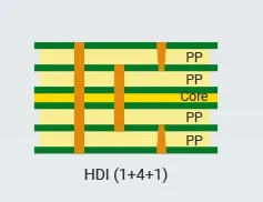
On sequential HDI builds the same rule is applied layer by layer. Laser vias that land on a plane are given thermal relief on the target layer only; the capture pad on the previous layer stays solid if it is not connected to a large pour. This keeps the via current capacity high while still controlling heat at the solder interface. Panel design also matters: we place the thermal-relief pads away from the panel edge and from high-density routing channels so that copper density remains balanced and warpage stays inside the 0.5 % limit. Process control adds a final check—after outer-layer etching the spoke width is measured at five locations per panel; any spoke that falls below 80 % of nominal triggers a hold for CAM review.
The reason these numbers work is simple: they keep the thermal resistance of the neck high enough that the solder joint reaches liquidus temperature within the reflow profile window, yet low enough that DC resistance does not rise above the value the circuit can tolerate. In practice the resistance increase is less than 5 mΩ for a four-spoke 0.12 mm design on 1/2 oz copper, which is acceptable for most power and ground nets on HDI boards.
When solid connections are left alone
Solid via-to-plane connections are accepted when the pad is purely a thermal via under a power device and no solder joint is formed on that pad, or when the net is a high-current path carrying more than 2 A continuous and the designer has already validated the temperature rise. In those cases we keep the solid copper but still enforce a minimum clearance to adjacent signal traces so that the plane does not create an unintended heat bridge to fine-pitch components. RF or high-speed differential pairs that share a plane connection are also left solid if the spoke would introduce an impedance discontinuity larger than the allowed 5 %. The trade-off is clear: thermal relief improves solderability at the cost of a small resistance and inductance increase; solid copper preserves electrical performance at the cost of tighter process control during assembly. When the customer supplies measured thermal data or a validated current profile, the factory follows that data rather than the default spoke rule.
In short, HDI thermal relief is applied wherever a solder joint must form against a large copper mass. The spokes are sized to the copper weight and via geometry that the sequential process can actually hold, and the decision is locked in at CAM so that every panel leaving the factory carries the same controlled heat path.