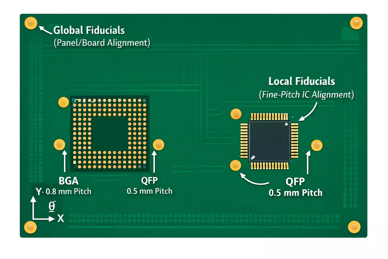
In our CAM review for HDI boards we treat HDI fiducial placement as a hard gate before panel release. Global fiducials are placed first in an L-pattern at three corners, then local fiducials are added beside every BGA or dense SMT zone that exceeds roughly 15 × 15 mm. The rule is non-negotiable on production panels because the SMT lines we feed cannot maintain the required placement accuracy without them. We either insert the missing marks ourselves or stop the job and send a DFM note back.

Registration stack-up and copper balance push the need for extra reference points
HDI sequential lamination builds the board in multiple press cycles. Each cycle adds a small but measurable shift between the core and the outer build-up layers. Laser vias and microvia stacks amplify that shift because the laser drills to a copper capture pad that itself may have moved. At the same time copper density is rarely uniform across an HDI design; high-density zones expand and contract differently from sparse areas during reflow. The net result is that the absolute position of a fine-pitch BGA relative to the board outline can drift by 50–80 µm from the CAD data. SMT cameras that only see the board outline or a single pair of marks cannot correct for that local movement. That is why the factory insists on local fiducials placed within 5–10 mm of the package edge—they give the placement head a fresh optical zero that is still valid after the board has gone through the reflow profile.
Material thickness also matters. On 0.4 mm or thinner HDI cores the panel is more flexible; conveyor vibration and vacuum hold-down on the SMT machine introduce additional short-term distortion. A global fiducial set that sits 100 mm away from the BGA no longer represents the local topography once the panel is clamped. Local marks solve that problem directly.
What the assembly line actually rejects when the marks are wrong
If the global set is incomplete or the local set is missing, the first symptom is not an electrical failure—it is a placement offset that only appears after the first reflow. BGAs show corner balls open or shorted; 0.4 mm pitch QFNs develop solder bridges on one side. The AOI system flags the defect, the board goes to rework, and the rework station then has to re-align to the same imperfect fiducial set, compounding the error. On a 500-piece panel we have seen first-pass yield drop 8–12 % solely from fiducial-related placement scatter. In extreme cases the entire panel is quarantined because the SMT program cannot lock onto a reliable optical reference and the line stops until a new program or a new set of boards arrives. Shipment dates slip by the length of that stoppage.
Solder-mask registration adds another failure mode. When the mask is printed after the copper image, any residual registration error can partially cover a fiducial that was drawn too close to a copper feature. The camera then sees an incomplete circle or an irregular edge and either rejects the board or forces a manual teach that is never as repeatable as a clean optical mark. That is why we enforce a 1.5–2.0 mm clear copper-free zone around every fiducial before the mask artwork is released.
CAM rules and panel-level compensation we apply before release
Standard production practice starts with three global fiducials of 1.0 mm diameter, copper-defined, with a 3.0 mm diameter mask opening. They sit at least 5 mm inside the board edge and 7 mm from any routing path so that the panel break-out does not damage them. The L-shape orientation is preferred because it gives the SMT vision system both X and Y references plus a rotation check. For every BGA or high-density SMT island larger than about 15 mm on a side we add a pair of local fiducials of the same size, placed 5–8 mm outside the package outline and clear of any copper or via. If the design already contains usable copper pads that meet size and clearance, we convert them rather than adding new copper; otherwise we insert new pads in the CAM database and regenerate the mask and legend layers.
On multi-image panels the same relative placement is repeated on every board so that the SMT program can be taught once and used across the whole panel. We also check that no fiducial falls under a tooling hole, a barcode, or a copper pour that would change after etching. When the design density is so high that space is scarce we reduce the local fiducial diameter to 0.8 mm and tighten the clear zone to 1.5 mm, but we never drop below two local marks per critical package. The finished artwork is then run through an automatic DFM check that measures the actual distance from each local mark to the nearest BGA corner; any value outside 5–12 mm is flagged for manual review.
These numbers are not arbitrary. They match the field of view and resolution of the cameras on the placement machines that receive our panels. A mark that is too far away forces the machine to use a less accurate global transform; a mark that is too close risks being covered by the component body after placement and becoming useless for any later inspection or rework step.
Situations where the factory accepts a reduced fiducial set
On very small form-factor HDI boards (under 20 × 20 mm) there is simply no real estate for three global marks plus locals. In those cases we accept two global fiducials placed on opposite corners and rely on the machine’s edge-detection capability for the third reference, provided the customer has confirmed that the SMT line can run with that configuration. Boards that contain only 0.5 mm pitch or coarser components and no BGA larger than 10 mm can also drop the local set; the global marks alone are then sufficient. When a customer supplies a proven placement program that already compensates for missing locals we release the panel as-is, but we still note the risk on the traveler so that any later yield issue is traced back to the agreed exception rather than to a CAM error. In every relaxed case the trade-off is the same: lower first-pass placement yield and higher rework cost if the board later moves to a different SMT line that does not have the same compensation data.
The practical limit is reached when the design has no usable free area at all. At that point we either recommend a slight board-size increase or accept that the assembly house will have to use a custom fixture and manual teach—both of which add cost and schedule risk that the factory cannot absorb.