Introduction
The rapid evolution of 5G and next-generation wireless networks has placed unprecedented demands on RF front-end modules. These critical subsystems handle power amplification, filtering, switching, and signal conditioning in base stations, small cells, and user equipment. At Aivon, we specialize in manufacturing advanced RF PCBs that enable high-performance 5G front-ends through optimized material selection, precise impedance control, thermal management, and high-density integration.
This article explores the development of 5G RF front-ends, key enabling technologies, duplexing methods, power device integration, and emerging applications such as satellite and lunar communications from a PCB engineering perspective.
Evolution of 5G RF Front-End Modules and PCB Requirements
5G RF front-ends have evolved from discrete component designs to highly integrated modules supporting massive MIMO, beamforming, and mmWave frequencies. Early 4G designs used simpler architectures, while 5G demands wider bandwidths, higher power efficiency, and multi-band operation.
PCB Design Implications:
- Higher Frequency Operation: Sub-6 GHz and mmWave (24-40 GHz+) bands require low-loss laminates (e.g., Rogers, Taconic, or high-performance FR4 hybrids) with stable dielectric constants and low dissipation factors to minimize insertion loss and signal attenuation.
- Dense Integration: Front-end modules integrate PAs, LNAs, switches, filters, and beamforming ICs. HDI technology with microvias, stacked vias, and fine-pitch routing enables compact layouts while maintaining signal integrity.
- Power and Thermal Challenges: 5G power amplifiers generate significant heat. Thick copper layers (2oz-4oz), thermal via arrays, embedded copper coins, and metal-core substrates are essential to dissipate heat and prevent performance degradation or reliability failures.
Market growth in 5G infrastructure continues to drive demand for PCBs that support higher efficiency and smaller form factors across base stations and customer premise equipment.
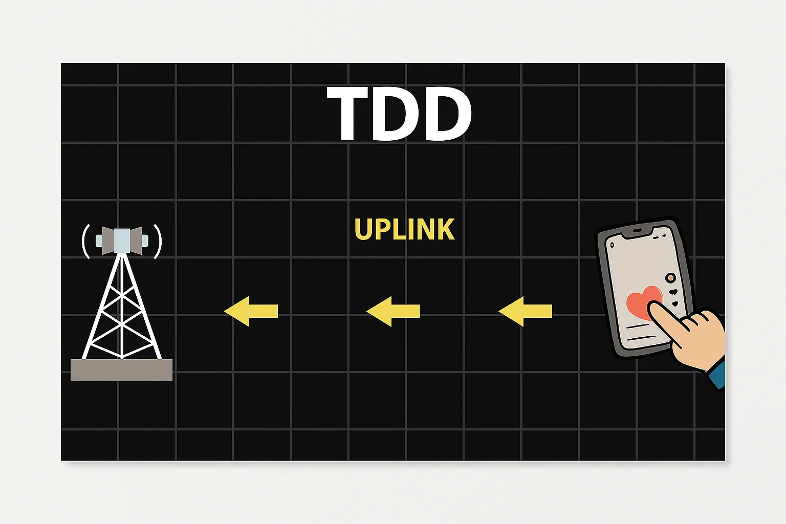
TDD vs FDD Duplexing: Impact on PCB Architecture
Time Division Duplexing (TDD) and Frequency Division Duplexing (FDD) define how uplink and downlink share spectrum.
- TDD: Uses the same frequency band for transmit and receive, separated in time. Dominant in many 5G deployments due to flexible spectrum allocation.
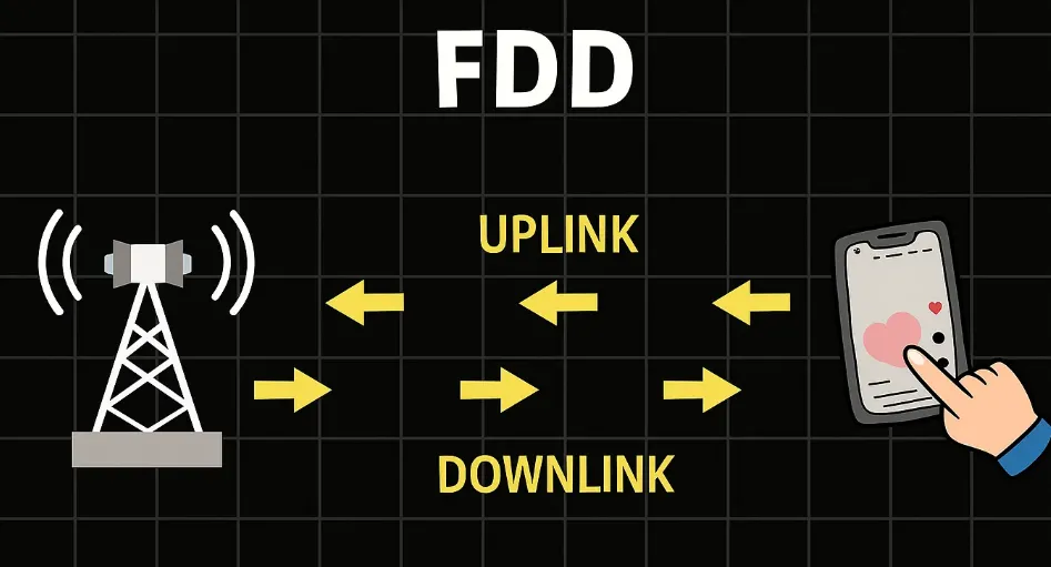
- FDD: Uses separate frequency bands for simultaneous transmit and receive, offering lower latency in some scenarios.
PCB Design Considerations:
- TDD Systems: Require fast RF switches and precise timing control. PCB layouts must minimize trace lengths between switches and antennas to reduce insertion loss and support rapid switching without introducing distortion.
- FDD Systems: Demand high-isolation duplexers and filters. Multilayer stack-ups with dedicated ground planes and via fencing are necessary to achieve the required port-to-port isolation and prevent self-interference.
- Hybrid Implementations: Many modern systems support both modes. Flexible PCB designs with segmented power domains and careful routing help manage the different filtering and switching requirements while controlling EMI.
RF Power Device Integration and PCB Optimization
Leading semiconductor solutions, such as those from NXP, offer integrated GaN and LDMOS devices optimized for 5G power amplification. These devices provide higher efficiency and power density compared to previous generations.
PCB Engineering Challenges:
- High-Current Paths: Power devices require wide traces, heavy copper planes, and optimized via arrays to handle peak currents while minimizing IR drop and inductance.
- Impedance Matching and Harmonic Control: Matching networks and harmonic filters must be placed close to the device. Precision etching and tight impedance tolerances (+/- 5%) ensure consistent performance across production volumes.
- Thermal Management: GaN devices run hot at high power levels. Advanced techniques like coin embedding, thermal interface materials, and balanced copper distribution prevent hotspots that could cause parametric drift or solder joint fatigue.
Digital Twins in 5G Telecommunications and PCB Development
Digital twin technology creates virtual replicas of physical systems for simulation, optimization, and predictive maintenance. In telecommunications, digital twins model entire networks, including RF front-ends, to predict performance under varying loads and environmental conditions.
PCB Relevance:
- Early digital twin integration allows simulation of signal integrity, thermal behavior, and EMI before physical prototyping. This reduces design iterations and improves first-pass success rates.
- PCB manufacturers can use twin-derived data to refine stack-up configurations, material choices, and via structures for specific 5G deployment scenarios.
- Predictive modeling helps anticipate reliability issues such as material degradation under thermal cycling or vibration in outdoor base stations.
High-Frequency Applications: Ka-Band and Satellite Communications
Ka-band (26-40 GHz) inter-satellite links, such as those used in the Iridium constellation, and emerging lunar relay systems demand even more stringent PCB performance.
Design Considerations:
- Low-Loss Transmission Lines: At Ka-band frequencies, material losses and surface roughness become dominant. Ultra-low-loss dielectrics and smooth copper foils are mandatory.
- Beamforming and Phased Arrays: Satellite and lunar relay antennas require large-scale integration of RF channels. Multilayer PCBs with precise length-matched routing and high-density interconnects support the necessary phase accuracy.
- Space and Harsh Environment Reliability: Vacuum, radiation, and extreme temperature swings in lunar applications require high-Tg materials, filled vias, and robust lamination processes to prevent delamination and outgassing.
These applications highlight the need for PCBs that bridge terrestrial 5G with non-terrestrial networks (NTN).
Advanced PCB Manufacturing Strategies for 5G RF Front-Ends
To meet the demands of modern wireless systems, manufacturers should focus on:
- Hybrid Stack-Ups: Combining standard FR4 with RF-specific laminates for cost-effective multi-band designs.
- Precision Fabrication: Laser drilling, back-drilled vias, and via-in-pad technology to minimize discontinuities in high-frequency paths.
- Thermal and Power Solutions: Copper balancing, embedded heat spreaders, and optimized PDN design for high-efficiency power amplification.
- Testing and Validation: Comprehensive VNA testing, thermal profiling, and reliability stress testing to ensure consistent performance in volume production.
- Cross-Industry Applications: Solutions developed for 5G infrastructure transfer effectively to automotive radar, industrial IoT, and aerospace systems.
Conclusion
The continued advancement of 5G RF front-end modules, combined with emerging duplexing techniques, power device integration, and satellite/lunar communication requirements, creates complex challenges for PCB designers. Success depends on expert management of signal integrity, thermal dissipation, material performance, and manufacturing precision.
At Aivon, our deep expertise in RF PCB fabrication helps customers overcome these hurdles, delivering reliable, high-performance boards for 5G infrastructure, satellite systems, and beyond. Early collaboration with an experienced manufacturer ensures your wireless designs achieve optimal efficiency, range, and long-term reliability in demanding real-world deployments.