Introduction
RF communication systems form the backbone of modern wireless technologies, including 5G, IoT, satellite links, radar, and industrial automation. The performance of these systems is largely determined by the quality of the RF front-end and supporting circuitry on the printed circuit board. At Aivon, we specialize in manufacturing complex RF PCBs that ensure signal integrity, low noise, high linearity, and thermal stability through advanced material selection, precise fabrication, and optimized stack-up design.
This article examines key RF circuit components, their functions, and the critical PCB design and manufacturing considerations required to achieve robust wireless performance.
RF Communication System Architecture and PCB Integration
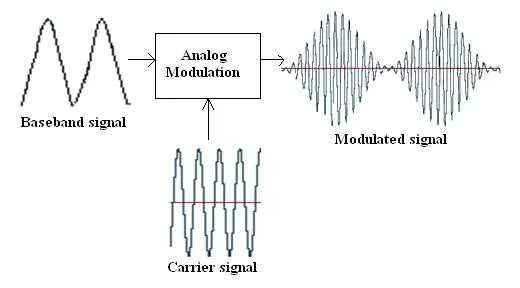
A typical RF system includes the transceiver, power amplifier, low-noise amplifier (LNA), filters, mixers, oscillators, and antenna interface. These elements work together in the RF front-end to handle signal transmission, reception, frequency conversion, and amplification.
PCB-Level Challenges:
- High-frequency signals are sensitive to impedance mismatches, parasitic inductance, and crosstalk. Multilayer stack-ups with dedicated RF layers, continuous ground planes, and careful routing are essential to maintain 50 ohms characteristic impedance throughout the signal chain.
- Power integrity becomes critical as amplifiers and mixers draw varying currents. Segmented power planes with multiple decoupling stages prevent voltage ripple from degrading system performance.
Passive Components in RF Circuits: Selection and Layout Impact
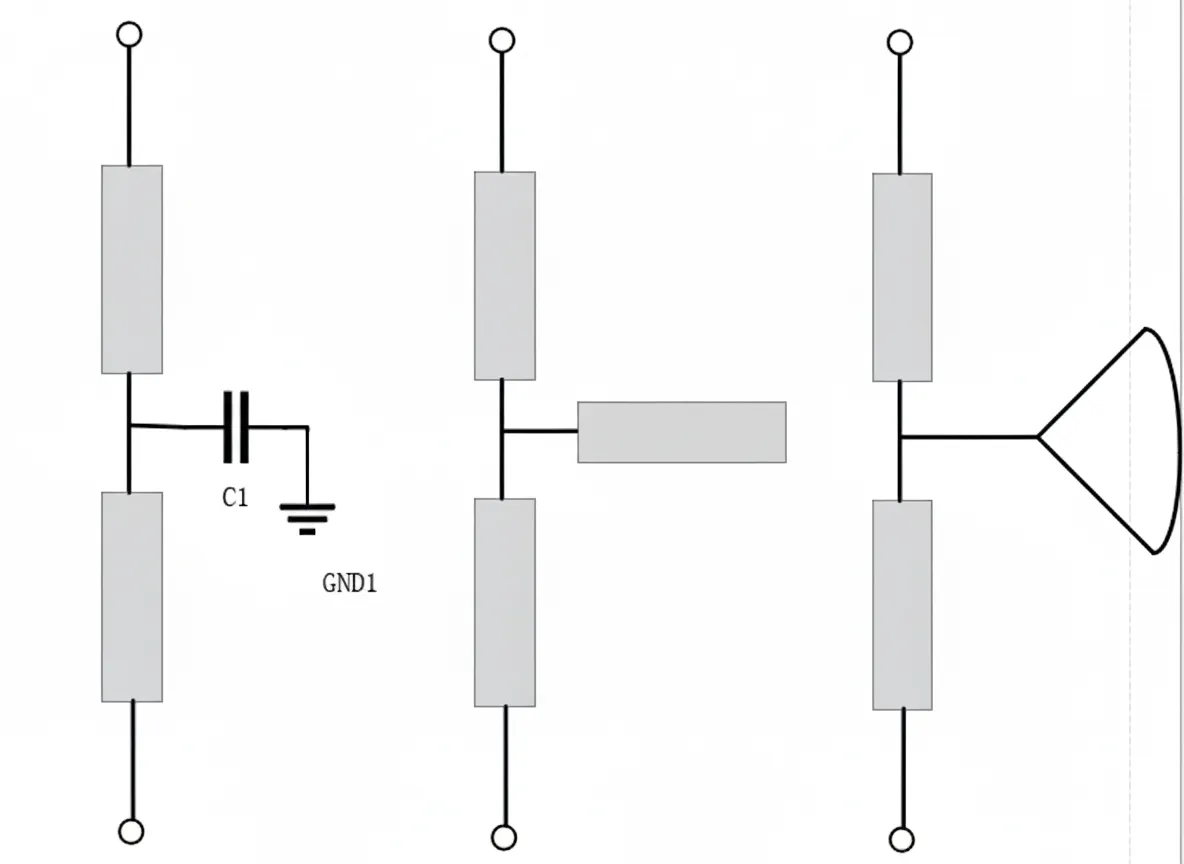
Passive components - resistors, capacitors, inductors, and transmission lines - play vital roles in matching networks, filtering, biasing, and coupling.
- Capacitors and Inductors: Used for DC blocking, RF bypassing, and resonant circuits.
- Resistors: Provide termination, attenuation, and biasing.
PCB Design Considerations:
- High-frequency performance requires components with low parasitic effects. Surface-mount devices (SMD) with small packages minimize inductance, but demand precise pad design and solder mask control during fabrication.
- Distributed elements such as microstrip lines, stubs, and coupled lines often replace discrete components at GHz frequencies. Accurate etching tolerances and dielectric thickness control are necessary to achieve target impedance and phase characteristics.
- Thermal expansion mismatch between components and substrate can cause reliability issues. High-Tg laminates with matched CTE improve long-term stability in harsh environments.
Active Components and RF Amplifiers on PCBs
Active devices, particularly MOS-based transistors, GaAs, GaN, and SiGe devices, provide amplification, switching, and mixing functions.
RF Amplifiers:
- Low Noise Amplifiers (LNAs) for receiver sensitivity
- Power Amplifiers (PAs) for transmission range
- Driver and buffer amplifiers
Key Performance Concerns:
- Intermodulation Distortion (IMD): Nonlinearities in amplifiers generate unwanted spectral products that interfere with adjacent channels. Third-order intercept point (IP3) is a critical metric.
- Gain, Linearity, and Efficiency Trade-offs: Higher linearity often reduces efficiency, increasing heat dissipation.
PCB Implications:
- Amplifier layouts require short, wide traces for high-current paths and excellent thermal management. Thick copper (2oz+), thermal vias arrays, and metal-core or coin-embedded substrates help dissipate heat from PAs while preventing thermal drift in sensitive LNAs.
- Bias networks and matching circuits must be placed close to the device to minimize parasitic effects. Fan microstrip structures and tapered lines are often used for broadband matching, requiring high-precision fabrication to control line geometry.
- Grounding is crucial. Multiple vias under device ground pads reduce source inductance and improve stability.
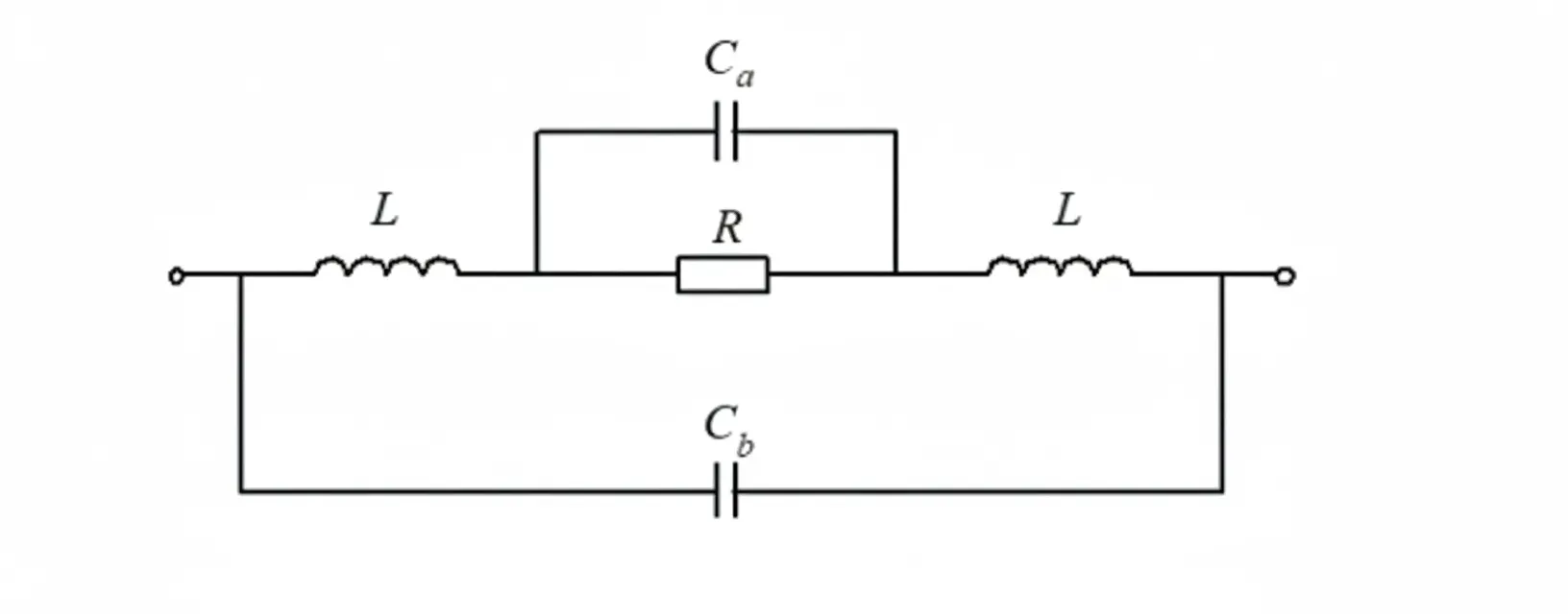
RF Filters and Front-End Design Requirements
RF filters are essential for rejecting out-of-band interference, selecting desired channels, and protecting receivers from strong blockers.
Common types include:
- Bandpass, low-pass, high-pass, and notch filters
- SAW, ceramic, and cavity filters for high selectivity
- Integrated passive filters using PCB transmission lines
Why Filters Matter:
They improve selectivity, reduce noise, and prevent intermodulation in crowded spectrum environments.
PCB Engineering Perspective:
- Filter performance depends heavily on substrate properties. Low-loss, stable dielectric materials minimize insertion loss and maintain sharp roll-off characteristics.
- Distributed filters (e.g., coupled line or hairpin resonators) require tight dimensional control and uniform copper thickness during etching and lamination.
- RF front-end integration often combines LNAs, filters, switches, and mixers in compact modules. HDI technology with microvias enables dense layouts while maintaining isolation between stages.
- Phase shift networks, such as 90-degree hybrids, are used for image rejection and balanced mixing. These demand precise length matching and symmetric routing to achieve accurate phase balance.
PCB Manufacturing Strategies for RF Circuit Reliability
To support demanding RF front-ends, manufacturers must address several critical aspects:
- Material Selection: Rogers, Taconic, or high-performance FR4 hybrids with low dissipation factor (Df) and stable dielectric constant (Dk) across frequency and temperature.
- Stack-Up Optimization: 6-16+ layers with dedicated ground and power planes for shielding, return paths, and EMI control. Hybrid constructions combine RF and digital sections effectively.
- Fabrication Precision: Tight impedance tolerances (plus or minus 5%), smooth copper profiles, back-drilled vias, and via-in-pad designs to reduce discontinuities.
- Thermal Management: Extensive use of copper pours, thermal vias, and embedded heat spreaders for power-hungry amplifiers.
- Signal Integrity: Controlled etching for transmission lines, via fencing for isolation, and compartmentalized shielding to minimize crosstalk and radiation.
- Reliability Enhancements: Filled vias, enhanced solder mask, and surface finishes like ENIG for long-term RF performance in automotive, telecom, and industrial applications.
These techniques help mitigate common failure modes such as solder joint fatigue under thermal cycling, material delamination, and performance drift due to manufacturing variations.
Conclusion
From passive matching networks and active amplifiers to critical front-end filters, every RF circuit component interacts intimately with the PCB. Successful wireless designs require expert attention to impedance control, thermal dissipation, material stability, and fabrication precision to translate theoretical performance into real-world reliability.
At Aivon, our advanced RF PCB manufacturing capabilities help engineers overcome these challenges across 5G infrastructure, IoT gateways, radar systems, and industrial wireless solutions. Early collaboration with an experienced manufacturer ensures your RF front-end designs achieve optimal signal integrity, linearity, and robustness in volume production.