










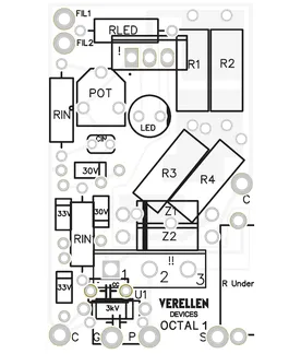
PCB Specifications
| Parameter | Value | Parameter | Value |
|---|---|---|---|
| PCB Type | Aluminum PCB | Quantity | 20 pcs |
| Layers | 2 Layers | Board Type | Single PCB |
| Dimensions | 30.1 x 49.91 mm | Copper Weight | 1oz |
| Thickness | 1.6 mm | Min Track / Spacing | 10/10mil |
| Surface Finish | HASL Lead Free | Min Hole Size | 1.5mm↑ |
| Solder Mask | White | Silkscreen | Black |
| Thermal Conductivity | 1.0W | Voltage Withstand | AC3000V |
Manufacturing Timeline
Logistics Information
Key Manufacturing Processes
Manufacturing Summary
These 20 aluminum boards were produced as individual boards measuring 30.1 × 49.91 mm with 1.6 mm total thickness, 1 oz copper, and 1.0W thermal conductivity. The 2-layer stack-up required precise metal base preparation and thermal insulation lamination to deliver both AC 3000V isolation and effective heat transfer. With a standard 10/10 mil track spacing and minimum 1.5 mm hole size, the design presented conventional geometry that allowed stable etching and drilling while maintaining the aluminum substrate's thermal performance.
White solder mask and black silkscreen were applied after circuit imaging and etching. The HASL Lead Free surface finish was formed through molten solder coating and hot air leveling, yielding a flat, uniform coating compatible with the aluminum core. Heat dissipation control was monitored at each thermal stage to prevent warping or delamination, ensuring the finished boards retained their designed conductivity and mechanical stability.
Electrical testing verified voltage withstand and continuity on every board. The full sequence from engineering review through final inspection was completed in 4.1 days, producing a consistent set of aluminum PCBs that meet the customer's thermal and high-voltage requirements.
Explore More PCB Manufacturing Resources
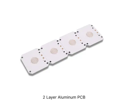
2 Layer Aluminum PCB Manufacturing Insights
Discover how AIVON manufactures 2 Layer Aluminum PCBs, including metal core structures, thermal management requirements, dielectric layer control, manufacturing challenges, and real production experience from customer orders.
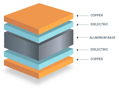
Engineering Challenges in 2 Layer Aluminum PCB Manufacturing: DFM and Thermal Issues
Explore common engineering queries in 2 layer aluminum PCB manufacturing, including CTE mismatch, thermal via design, dielectric bonding, and solder mask registration issues. Learn practical DFM solutions to reduce warpage, improve thermal performance, and increase production yield.
Real Production Records
| Order ID | PCB Type | Layers | Dimensions | Solder Mask | Surface Finish | Quantity | Action |
|---|---|---|---|---|---|---|---|
| ALU-20260727-042 | Aluminum PCB | 2 | 30.1 x 49.91 | White | HASL Lead Free | 120 | View detail |
| ALU-20260715-003 | Aluminum PCB | 1 | 482 x 44 | Black | HASL Lead Free | 5 | View detail |
| ALU-20260531-057 | Aluminum PCB | 1 | 378.5 x 220.5 | Black | HASL Lead Free | 125 | View detail |


