










PCB Specifications
| Parameter | Value | Parameter | Value |
|---|---|---|---|
| PCB Type | Flexible PCB | Quantity | 1000 pcs |
| Layers | 1 Layers | Board Type | Single PCB |
| Dimensions | 79.37 x 6.35 mm | Copper Weight | 1/2OZ |
| Thickness | 0.1 mm | Min Track / Spacing | 6/6mil↑ |
| Surface Finish | ENIG (Immersion Gold) | Min Hole Size | 0.3mm↑ |
| Solder Mask | None | Silkscreen | White |
| Material | Rolled Copper | Stiffener | None |
| Blind/Buried Vias | No |
Manufacturing Timeline
Logistics Information
Key Manufacturing Processes
Manufacturing Summary
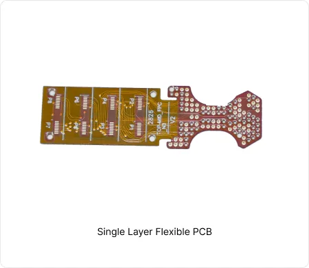
This production record covers 1000 single-layer flexible PCBs built on 0.1 mm polyimide with rolled copper at 1/2 oz weight. Each board measures 79.37 × 6.35 mm, creating a long, narrow strip format with 0.3 mm minimum hole size and standard 6/6 mil trace spacing. No soldermask or stiffener was applied; instead, white silkscreen and immersion gold ENIG surface finish were specified on exposed copper. The thin construction and flexible material required controlled polyimide handling and imaging to maintain flatness and registration throughout etching.
Coverlay lamination followed circuit definition to protect conductors while leaving pads open for plating. Electroless nickel deposition and immersion gold plating were completed in sequence, after which each panel underwent dynamic flex testing to confirm bend endurance. Batch AOI inspection, electrical testing, and yield tracking verified uniformity across the full quantity. The five-day schedule kept all process steps aligned without deviation from the specified parameters.
The completed flexible circuits exhibited consistent trace definition and plating adhesion, supporting reliable performance in the intended application.
Explore More PCB Manufacturing Resources
Real Production Records
| Order ID | PCB Type | Layers | Dimensions | Solder Mask | Surface Finish | Quantity | Action |
|---|---|---|---|---|---|---|---|
| FPC-20260821-065 | Flexible PCB | 4 | 111.25 x 16.75 | Yellow | ENIG (Immersion Gold) | 5 | View detail |
| FPC-20260819-026 | Flexible PCB | 4 | 59.8 x 65.5 | Yellow | ENIG (Immersion Gold) | 25 | View detail |
| FPC-20260810-032 | Flexible PCB | 4 | 357 x 45.8 | Black | ENIG (Immersion Gold) | 1000 | View detail |


