










PCB Specifications
| Parameter | Value | Parameter | Value |
|---|---|---|---|
| PCB Type | Flexible PCB | Quantity | 300 pcs |
| Layers | 2 Layers | Board Type | Panel PCB |
| Dimensions | 23 x 97 mm | Copper Weight | 1OZ |
| Thickness | 0.2 mm | Min Track / Spacing | 6/6mil↑ |
| Surface Finish | ENIG (Immersion Gold) | Min Hole Size | 0.3mm↑ |
| Solder Mask | Yellow | Silkscreen | White |
| Material | Rolled Copper | Stiffener | PI Stiffener |
Manufacturing Timeline
Logistics Information
Key Manufacturing Processes
Manufacturing Summary
This production record covered 300 panels of 2-layer flex PCBs built on 0.2 mm rolled copper polyimide. Measuring 23 x 97 mm, each board received PI stiffeners for localized rigidity while carrying a yellow soldermask, white silkscreen, and immersion gold ENIG finish. The thin construction and material choice required exact control during lamination and plating to preserve flex characteristics and surface integrity.
Polyimide material handling formed the initial focus, followed by circuit imaging and etching at standard 6/6 mil geometry. Coverlay lamination preceded solder mask application, after which electroless nickel deposition and immersion gold plating created the final ENIG surface. Process parameters stayed aligned with the 0.3 mm minimum hole size and overall panel layout throughout.
Dynamic flex testing assessed endurance under repeated bending, with AOI inspection and electrical testing confirming performance across the full quantity. All boards met specifications without deviation, completing the manufacturing cycle in 5.7 days.
Explore More PCB Manufacturing Resources
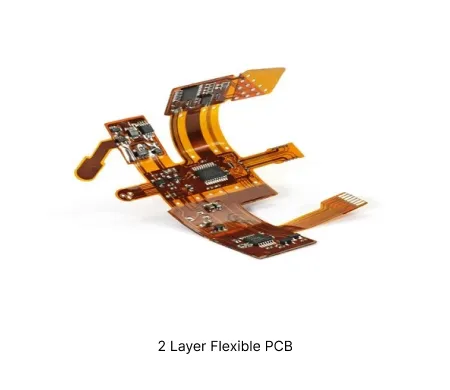
2 Layer Flexible PCB Manufacturing Insights
Discover how AIVON manufactures 2 Layer Flexible PCBs, including flexible material handling, multilayer flex structures, bending reliability requirements, manufacturing challenges, and real production experience from customer orders.
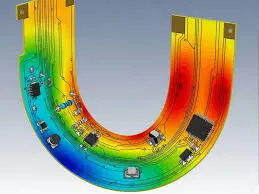
How to Prevent Engineering Queries in 2-Layer Flexible PCB Design
Explore engineering queries (EQ) in 2 layer flexible PCB manufacturing, including key DFM challenges such as bend design, coverlay alignment, via reliability, and copper balance. Practical insights help improve flexibility performance and production yield.
Real Production Records
| Order ID | PCB Type | Layers | Dimensions | Solder Mask | Surface Finish | Quantity | Action |
|---|---|---|---|---|---|---|---|
| FPC-20260821-065 | Flexible PCB | 4 | 111.25 x 16.75 | Yellow | ENIG (Immersion Gold) | 5 | View detail |
| FPC-20260819-026 | Flexible PCB | 4 | 59.8 x 65.5 | Yellow | ENIG (Immersion Gold) | 25 | View detail |
| FPC-20260810-032 | Flexible PCB | 4 | 357 x 45.8 | Black | ENIG (Immersion Gold) | 1000 | View detail |


