











PCB Specifications
| Parameter | Value | Parameter | Value |
|---|---|---|---|
| PCB Type | Flexible PCB | Quantity | 4500 pcs |
| Layers | 2 Layers | Board Type | Panel PCB |
| Dimensions | 318.2 x 8.5 mm | Copper Weight | 1OZ |
| Thickness | 0.2 mm | Min Track / Spacing | 6/6mil↑ |
| Surface Finish | ENIG (Immersion Gold) | Min Hole Size | 0.3mm↑ |
| Solder Mask | White | Silkscreen | None |
| Material | Rolled Copper | Stiffener | None |
Manufacturing Timeline
Logistics Information
Key Manufacturing Processes
Manufacturing Summary
Production of these 4500 flexible PCBs centered on 2-layer panels using 0.2 mm thick polyimide with rolled copper foil. Each panel measured 318.2 × 8.5 mm, creating long, narrow circuits that required careful material handling to preserve flatness and bend characteristics. Minimum 6/6 mil geometry, 0.3 mm holes, white soldermask, and immersion gold ENIG finish were applied without stiffeners, keeping the construction fully flexible while meeting the specified electrical and surface requirements.
After engineering review, polyimide sheets were prepared and imaged, followed by precise etching and coverlay lamination. White solder mask was then selectively applied before electroless nickel and immersion gold deposition to ensure solderable pads with stable nickel thickness. Process controls focused on maintaining uniform plating and adhesion across the extended panel length, avoiding wrinkles or registration drift common in thin flex substrates of this proportion.
Dynamic flex testing, batch AOI, and 100% electrical testing verified continuity and insulation integrity after coverlay and mask steps. The full run completed in 7.9 days with stable yields, delivering panels that consistently performed to the mechanical and electrical criteria of the order.
Explore More PCB Manufacturing Resources
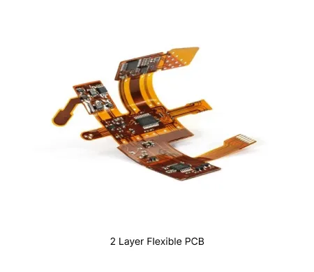
2 Layer Flexible PCB Manufacturing Insights
Discover how AIVON manufactures 2 Layer Flexible PCBs, including flexible material handling, multilayer flex structures, bending reliability requirements, manufacturing challenges, and real production experience from customer orders.
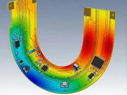
How to Prevent Engineering Queries in 2-Layer Flexible PCB Design
Explore engineering queries (EQ) in 2 layer flexible PCB manufacturing, including key DFM challenges such as bend design, coverlay alignment, via reliability, and copper balance. Practical insights help improve flexibility performance and production yield.
Real Production Records
| Order ID | PCB Type | Layers | Dimensions | Solder Mask | Surface Finish | Quantity | Action |
|---|---|---|---|---|---|---|---|
| FPC-20260821-065 | Flexible PCB | 4 | 111.25 x 16.75 | Yellow | ENIG (Immersion Gold) | 5 | View detail |
| FPC-20260819-026 | Flexible PCB | 4 | 59.8 x 65.5 | Yellow | ENIG (Immersion Gold) | 25 | View detail |
| FPC-20260810-032 | Flexible PCB | 4 | 357 x 45.8 | Black | ENIG (Immersion Gold) | 1000 | View detail |


