










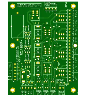
PCB Specifications
| Parameter | Value | Parameter | Value |
|---|---|---|---|
| PCB Type | FR4 PCB | Quantity | 15 pcs |
| Layers | 2 Layers | Board Type | Single PCB |
| Dimensions | 177.8 x 234.95 mm | Copper Weight | 4oz |
| Thickness | 1.6 mm | Min Track / Spacing | 10/10mil |
| Surface Finish | ENIG (Immersion Gold) | Min Hole Size | 0.3mm↑ |
| Solder Mask | Green | Silkscreen | White |
| Stack-up | Default | Impedance Control | No |
Manufacturing Timeline
Logistics Information
Key Manufacturing Processes
Manufacturing Summary
This production involved 15 units of 2-layer FR4 PCBs with 4 oz copper weight, board dimensions of 177.8 x 234.95 mm, and standard 1.6 mm thickness. Due to the heavy copper, the process incorporated thick copper electroplating and controlled copper etching to achieve the 10/10 mil track and spacing. These steps received close attention to ensure uniform thickness and accurate feature definition on the sizable boards.
Green solder mask and white silkscreen were applied, followed by electroless nickel and immersion gold deposition to create the ENIG surface finish. All boards then underwent electrical testing as part of the standard verification. The complete manufacturing cycle required 6.2 days.
Without impedance control or blind vias, the execution centered on delivering consistent heavy copper PCB layers and reliable plating adhesion. The chosen parameters and processes produced boards aligned with the specified requirements for current handling and connectivity.
Explore More PCB Manufacturing Resources
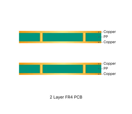
2 Layer FR4 PCB Manufacturing Insights
Discover how AIVON manufactures 2 Layer FR4 PCBs, including double-sided circuit structures, reliable through-hole fabrication processes, manufacturing challenges, and real production experience from customer orders.
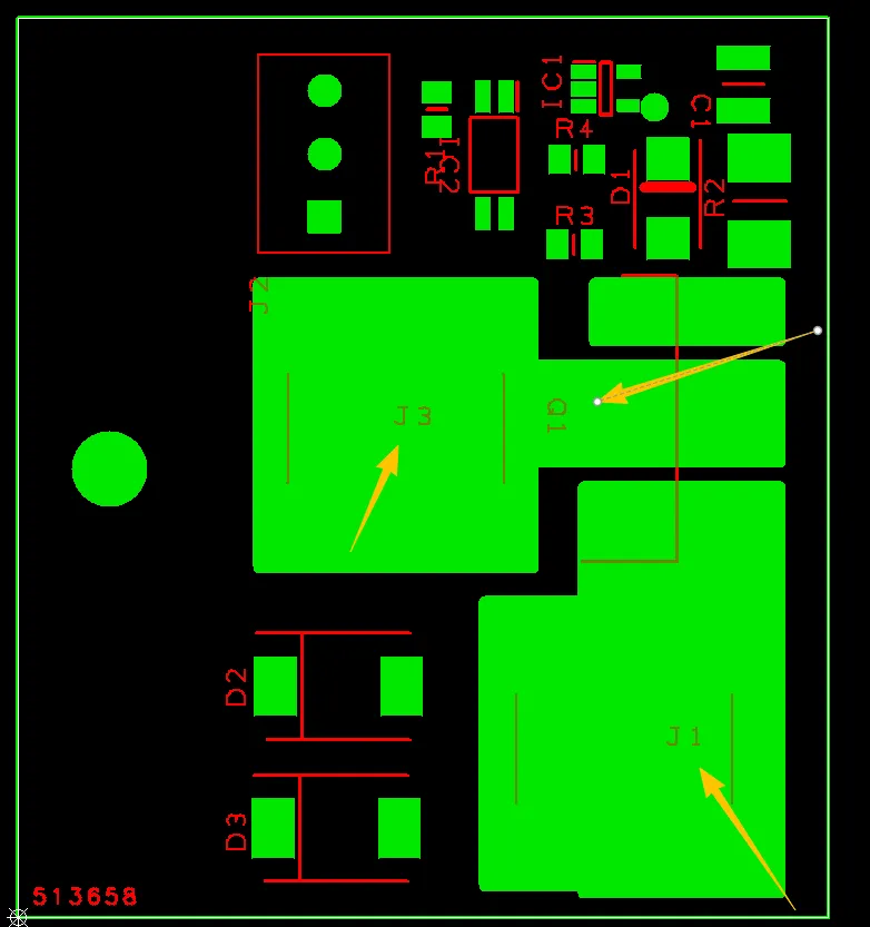
Common Engineering Queries in 2 Layer FR4 PCB Design and Manufacturing
Real Engineering Queries (EQ) and DFM issues for 2 Layer FR4 PCB (double-sided boards) from actual production reviews. Learn how to avoid common problems with via treatment, silkscreen on pads, solder mask openings, hole attributes, board edge clearance, and other frequent design pitfalls.
Real Production Records
| Order ID | PCB Type | Layers | Dimensions | Solder Mask | Surface Finish | Quantity | Action |
|---|---|---|---|---|---|---|---|
| FR4-20260910-004 | FR4 PCB | 2 | 69.92 x 69.91 | White | HASL Lead Free | 5 | View detail |
| FR4-20260907-001 | FR4 PCB | 2 | 90 x 40 | Green | HASL Lead Free | 30 | View detail |
| FR4-20260905-007 | FR4 PCB | 2 | 42.8 x 38.8 | Green | HASL Lead Free | 5 | View detail |


