










PCB Specifications
| Parameter | Value | Parameter | Value |
|---|---|---|---|
| PCB Type | FR4 PCB | Quantity | 210 pcs |
| Layers | 8 Layers | Board Type | Panel PCB |
| Dimensions | 130 x 202 mm | Copper Weight | 1oz |
| Thickness | 1.6 mm | Min Track / Spacing | 6/6mil↑ |
| Surface Finish | ENIG (Immersion Gold) | Min Hole Size | 0.25mm |
| Solder Mask | Green | Silkscreen | White |
| Stack-up | Custom | Impedance Control | Yes |
| Blind/Buried Vias | No |
Manufacturing Timeline
Logistics Information
Key Manufacturing Processes
Manufacturing Summary
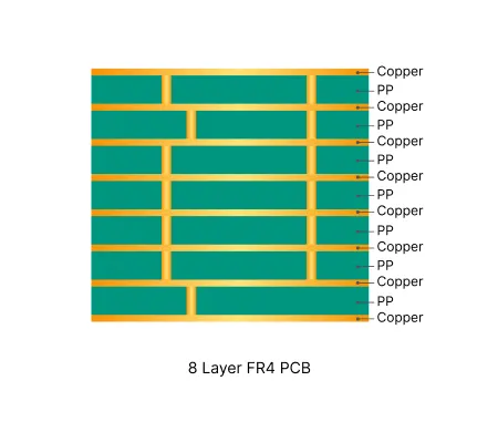
This 8-layer FR-4 board measured 130 × 202 mm at 1.6 mm thickness with 1 oz copper throughout and TG150 material. The 210-piece order featured controlled impedance, ENIG surface finish, green solder mask, and via tenting. Panelization was single-board with V-scoring plus routing for separation. Impedance requirements and the provided stackup made this order distinct from standard multilayer runs.
CAM review identified multiple DFM concerns. Process edges contained sharp corners inaccessible to the router, risking residual protrusions on the finished board; adjustments were made to ensure clean contours. Stamp holes at 0.3 mm diameter posed ink intrusion and blocking risks during mask application, which were mitigated through process parameter confirmation. Silkscreen characters positioned too close to pads were shifted where possible or selectively removed with customer approval to maintain minimum 4 mil white oil bridge clearance and prevent mask encroachment. Impedance line identification issues in the working gerber and a calculated 2/3 ohm deviation on inner layers were resolved by cross-verifying the customer table against compensated traces before lamination.
Production confirmation followed these clarifications, with full electrical testing and impedance reporting completed within 14 days. The boards delivered with consistent electrical performance and mechanical quality. For further details on the impedance line verification and stackup compensation, see the related engineering case study.
Explore More PCB Manufacturing Resources
8 Layer FR4 PCB Manufacturing Insights
Discover how AIVON manufactures 8 Layer FR4 PCBs, including advanced multilayer structures, signal integrity requirements, impedance control, fabrication processes, manufacturing challenges, and real production experience from customer orders.

How to Avoid Common Engineering Queries in Multilayer FR4 PCB Design
Real multilayer FR4 PCB CAM review cases covering stack-up confirmation, impedance control, copper balance, via tenting, and edge clearance EQs. Discover practical DFM best practices for 4-layer and higher boards to reduce engineering queries, prevent warpage, and improve first-pass yield.
Real Production Records
| Order ID | PCB Type | Layers | Dimensions | Solder Mask | Surface Finish | Quantity | Action |
|---|---|---|---|---|---|---|---|
| FR4-20260918-033 | FR4 PCB | 6 | 55 x 41.7 | Green | ENIG (Immersion Gold) | 5 | View detail |
| FR4-20260912-059 | FR4 PCB | 2 | 275 x 193.7 | Green | ENIG (Immersion Gold) | 100 | View detail |
| FR4-20260819-043 | FR4 PCB | 10 | 157 x 140 | Blue | ENIG (Immersion Gold) | 100 | View detail |


