


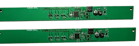
PCB Specifications
| Parameter | Value | Parameter | Value |
|---|---|---|---|
| PCB Type | FR4 PCB | Quantity | 25 pcs |
| Layers | 2 Layers | Board Type | Single PCB |
| Dimensions | 138.7 x 65.9 mm | Copper Weight | 1oz |
| Thickness | 1.6 mm | Min Track / Spacing | 6/6mil↑ |
| Surface Finish | HASL Lead Free | Min Hole Size | 0.8mm↑ |
| Solder Mask | None | Silkscreen | White |
| Stack-up | Custom | Impedance Control | No |
Manufacturing Timeline
Logistics Information
Key Manufacturing Processes
Manufacturing Summary
For this order of 25 single 2-layer FR4 PCBs, production followed a custom stackup using 1.6 mm thickness and 1 oz copper on both sides. Boards measured 138.7 × 65.9 mm with standard 6/6 mil track and spacing together with 0.8 mm minimum holes. The absence of solder mask and impedance control allowed conventional process parameters during imaging and etching while directing attention to surface preparation for the white silkscreen applied directly to the laminate.
HASL Lead Free surface finish was achieved through molten solder coating and hot air leveling, tinning all exposed copper traces and pads without mask protection. This required sequenced handling after etching to maintain cleanliness and prevent oxidation before silkscreen application. The chosen finish and bare-board configuration suit applications needing direct soldering or probe access, and all parameters stayed within proven process windows.
Engineering review, material preparation, circuit imaging, etching, and electrical testing were completed in 1.6 days. Every board passed continuity and isolation checks, confirming reliable electrical performance and consistent feature accuracy across the full set.
This order also received positive feedback from the customer regarding the consistent quality and reliable delivery. View the full customer review→
Explore More PCB Manufacturing Resources
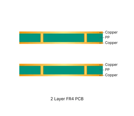
2 Layer FR4 PCB Manufacturing Insights
2 layer FR4 PCBs deliver cost-effective solutions for most electronic designs. Their simple structure enables consistent quality and efficient production cycles.
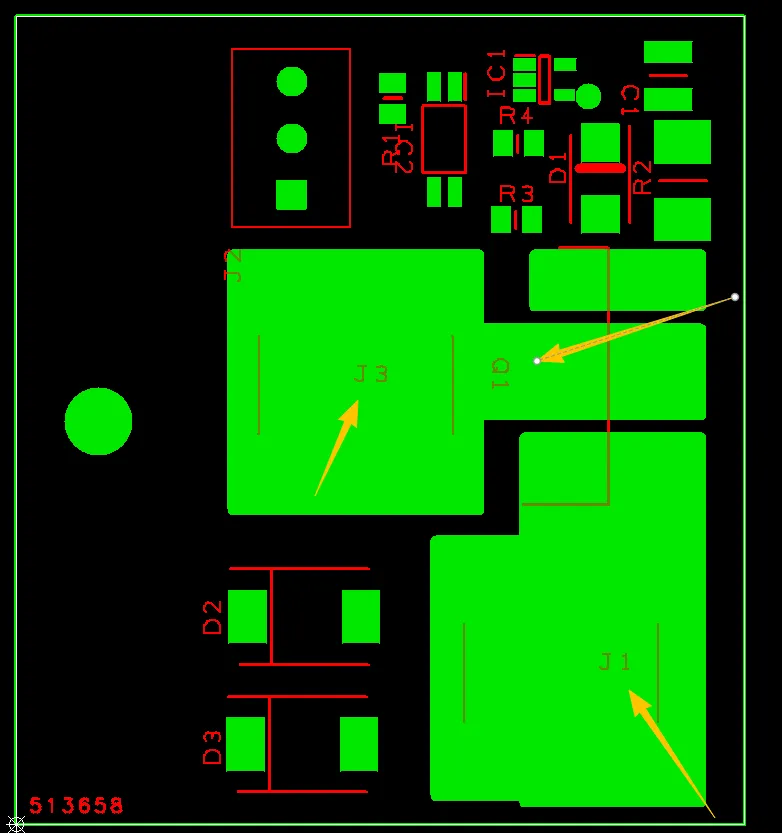
Common Engineering Queries in 2 Layer FR4 PCB Design and Manufacturing
Real Engineering Queries (EQ) and DFM issues for 2 Layer FR4 PCB (double-sided boards) from actual production reviews. Learn how to avoid common problems with via treatment, silkscreen on pads, solder mask openings, hole attributes, board edge clearance, and other frequent design pitfalls.
Real Production Records
| Order ID | PCB Type | Layers | Dimensions | Solder Mask | Surface Finish | Quantity | Action |
|---|---|---|---|---|---|---|---|
| FR4-20261009-004 | FR4 PCB | 1 | 58.85 x 65.86 | Green | HASL Lead Free | 50 | View detail |
| FR4-20261007-048 | FR4 PCB | 2 | 99.04 x 75.87 | Matte Black | HASL Lead Free | 15 | View detail |
| FR4-20261007-047 | FR4 PCB | 2 | 92.84 x 72.52 | Green | HASL Lead Free | 5 | View detail |


