


PCB Specifications
| Parameter | Value | Parameter | Value |
|---|---|---|---|
| PCB Type | FR4 PCB | Quantity | 5 pcs |
| Layers | 2 Layers | Board Type | Panel PCB |
| Dimensions | 99 x 159.5 mm | Copper Weight | 1oz |
| Thickness | 1.6 mm | Min Track / Spacing | 10/10mil |
| Surface Finish | HASL Lead Free | Min Hole Size | 0.3mm↑ |
| Solder Mask | Green | Silkscreen | White |
| Stack-up | Custom | Impedance Control | No |
Manufacturing Timeline
Logistics Information
Key Manufacturing Processes
Manufacturing Summary
This order comprised five 2-layer FR4 panel PCBs measuring 99 × 159.5 mm, built to a 1.6 mm thickness with 1 oz copper. The 10/10 mil track and spacing qualified as standard geometry, paired with a 0.3 mm minimum hole size and custom stackup. Engineering review and material preparation confirmed material compatibility before circuit imaging, etching, and plating proceeded without deviation.
Green solder mask and white silkscreen were applied in sequence, followed by lead-free HASL surface finish. Molten solder coating and hot air leveling produced an even, oxidation-resistant coating suited to the panel format and subsequent assembly needs. Full electrical testing verified net continuity and isolation on every panel.
The complete cycle took 2.6 days and delivered panels that met all specified tolerances for this conventional 2-layer configuration. Process parameters remained stable throughout, resulting in consistent board quality and reliable solderability for the customer's low-volume requirement.
This order also received positive feedback from the customer regarding the consistent quality and reliable delivery. View the full customer review→
Explore More PCB Manufacturing Resources
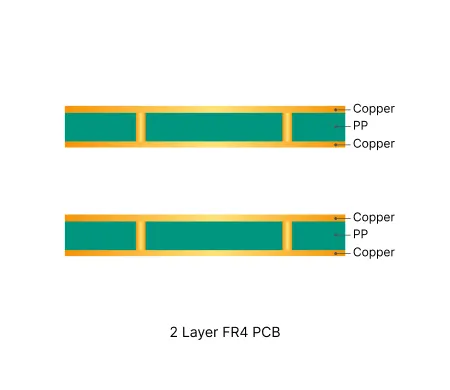
2 Layer FR4 PCB Manufacturing Insights
Discover how AIVON manufactures 2 Layer FR4 PCBs, including double-sided circuit structures, reliable through-hole fabrication processes, manufacturing challenges, and real production experience from customer orders.
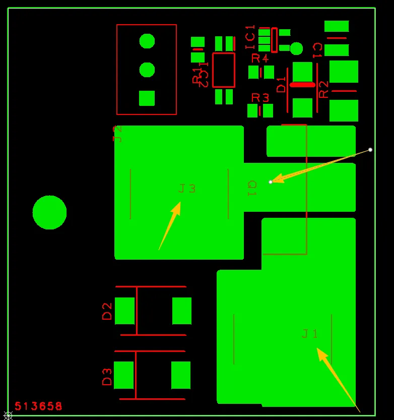
Common Engineering Queries in 2 Layer FR4 PCB Design and Manufacturing
Real Engineering Queries (EQ) and DFM issues for 2 Layer FR4 PCB (double-sided boards) from actual production reviews. Learn how to avoid common problems with via treatment, silkscreen on pads, solder mask openings, hole attributes, board edge clearance, and other frequent design pitfalls.
Real Production Records
| Order ID | PCB Type | Layers | Dimensions | Solder Mask | Surface Finish | Quantity | Action |
|---|---|---|---|---|---|---|---|
| FR4-20261009-004 | FR4 PCB | 1 | 58.85 x 65.86 | Green | HASL Lead Free | 50 | View detail |
| FR4-20261007-048 | FR4 PCB | 2 | 99.04 x 75.87 | Matte Black | HASL Lead Free | 15 | View detail |
| FR4-20261007-047 | FR4 PCB | 2 | 92.84 x 72.52 | Green | HASL Lead Free | 5 | View detail |


