










PCB Specifications
| Parameter | Value | Parameter | Value |
|---|---|---|---|
| PCB Type | FR4 PCB | Quantity | 5 pcs |
| Layers | 2 Layers | Board Type | Single PCB |
| Dimensions | 42.67 x 26.55 mm | Copper Weight | 1oz |
| Thickness | 1.6 mm | Min Track / Spacing | 10/10mil |
| Surface Finish | HASL Lead Free | Min Hole Size | 0.5mm |
| Solder Mask | Green | Silkscreen | White |
| Stack-up | Custom | Impedance Control | No |
Manufacturing Timeline
Logistics Information
Key Manufacturing Processes
Manufacturing Summary
The manufacturing of these five 2-layer FR4 boards began with a thorough engineering review of the custom stackup and specifications, including the compact dimensions of 42.67 x 26.55 mm and standard 1.6 mm thickness. With 1 oz copper layers and a conventional 10/10 mil track-to-spacing ratio, the circuit imaging and etching processes were carried out using established parameters to achieve clean traces and accurate feature definition on the single boards.
We applied green solder mask and white silkscreen before proceeding to the lead-free HASL surface finish. This involved molten solder coating followed by hot air leveling to create a uniform protective layer on the exposed copper, ensuring excellent solderability for the 0.5 mm minimum hole size. Each board then underwent comprehensive electrical testing to verify netlist compliance.
Completed in 2.2 days, this small production run demonstrated reliable execution from material preparation through final inspection. The straightforward design without impedance control or blind vias allowed us to focus on delivering boards with consistent surface quality and dimensional stability suited for general electronic applications.
This order also received positive feedback from the customer regarding the consistent quality and reliable delivery. View the full customer review→
Explore More PCB Manufacturing Resources
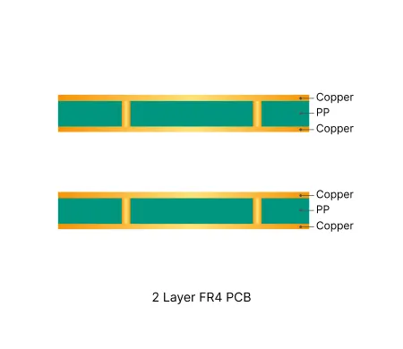
2 Layer FR4 PCB Manufacturing Insights
Discover how AIVON manufactures 2 Layer FR4 PCBs, including double-sided circuit structures, reliable through-hole fabrication processes, manufacturing challenges, and real production experience from customer orders.
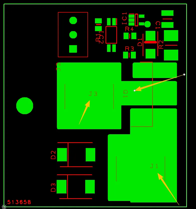
Common Engineering Queries in 2 Layer FR4 PCB Design and Manufacturing
Real Engineering Queries (EQ) and DFM issues for 2 Layer FR4 PCB (double-sided boards) from actual production reviews. Learn how to avoid common problems with via treatment, silkscreen on pads, solder mask openings, hole attributes, board edge clearance, and other frequent design pitfalls.
Real Production Records
| Order ID | PCB Type | Layers | Dimensions | Solder Mask | Surface Finish | Quantity | Action |
|---|---|---|---|---|---|---|---|
| FR4-20260928-023 | FR4 PCB | 1 | 90.5 x 117.5 | Green | HASL Lead Free | 100 | View detail |
| FR4-20260923-016 | FR4 PCB | 2 | 100 x 87 | Blue | HASL Lead Free | 5 | View detail |
| FR4-20260919-046 | FR4 PCB | 2 | 76 x 374 | Matte Black | HASL Lead Free | 30 | View detail |


