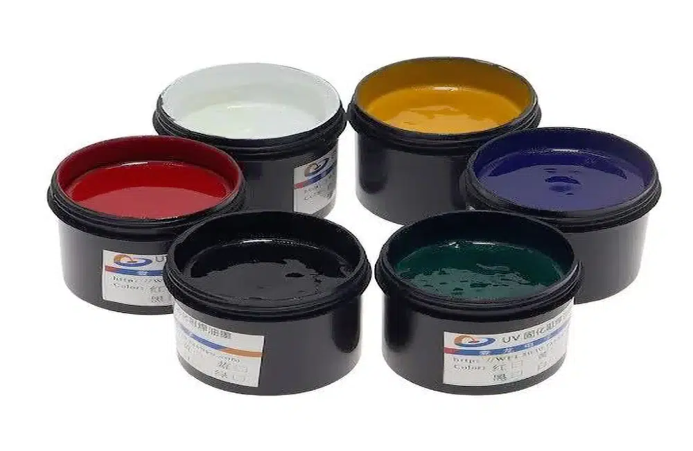
dry-film-solder-mask
Dry film solder mask serves as a critical protective layer in printed circuit board (PCB) manufacturing, shielding copper traces from oxidation, preventing solder bridges during assembly, and enhancing overall board durability. This tag, Dry Film Solder Mask, encompasses a collection of articles that delve into its composition, application techniques, and advantages over traditional liquid solder masks. For engineers, hobbyists, and manufacturers searching for reliable information on this topic, these resources provide essential guidance on achieving precise, uniform coverage that meets industry standards like IPC-SM-840. Understanding dry film solder mask begins with its photosensitive properties, which allow for high-resolution patterning through exposure and development processes. Users often seek practical advice on laminating the film onto PCBs, optimizing exposure times to avoid under- or over-exposure, and selecting the right film thickness for specific board designs. Best practices include ensuring a clean substrate surface prior to application to prevent adhesion issues, and using controlled environments to minimize defects such as bubbles or wrinkles. Compared to liquid masks, dry film offers superior edge definition and consistency, making it ideal for high-density interconnects in consumer electronics, automotive systems, and medical devices. For those troubleshooting common problems like poor adhesion or incomplete curing, our articles outline step-by-step solutions, including equipment recommendations and material compatibility checks. Whether you are prototyping a new circuit or scaling up production, exploring the content under this tag can help refine your processes, reduce rework, and improve yield rates. Readers interested in related PCB fabrication topics will find valuable connections to discussions on etching methods, via filling, and surface finishes that complement solder mask application.
Technical Articles
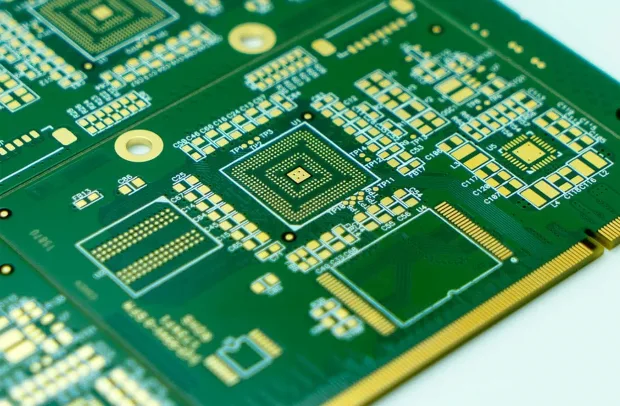
The Ultimate Guide to Selecting the Right Dry Film Solder Mask Thickness for Optimal PCB Performance
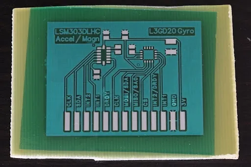
Mastering the Dry Film Solder Mask Exposure Process: A Step by Step Tutorial
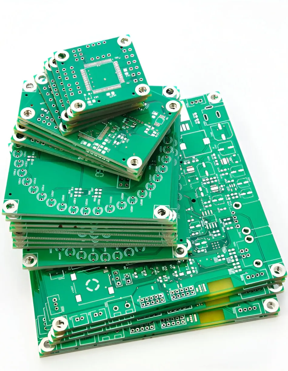
Dry Film vs. LPI Solder Mask: Which Is Right for Your PCB Project?
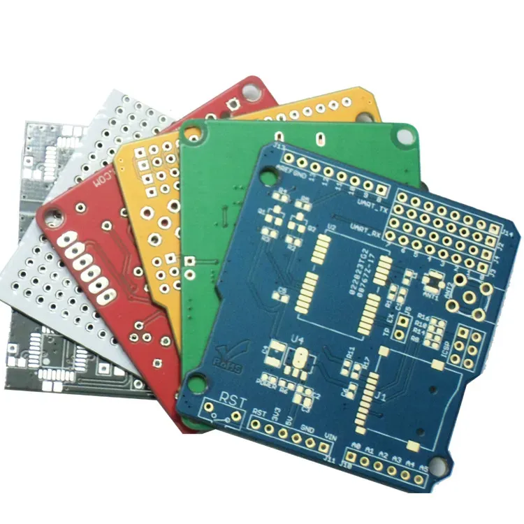
Understanding Solder Mask: A Beginner's Guide to PCB Protection
Get in Touch
Send Message
- Products & Service
- Company
- About AIVON
- Contact
- News
- Blog
- Certification
-


- Payment
-


2026 AIVON.COM All Rights Reserved