microvia-defects
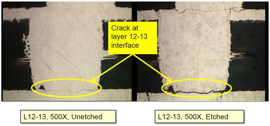
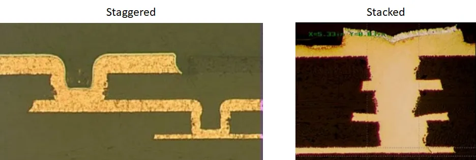
Microvias are essential components in modern printed circuit boards (PCBs), enabling high-density interconnections in multilayer designs. However, microvia defects can compromise the reliability and performance of electronic assemblies, leading to failures in critical applications such as consumer electronics, automotive systems, and aerospace equipment. This tag page on Microvia Defects gathers in-depth resources to help engineers, designers, and manufacturers identify, analyze, and mitigate these issues effectively. Common microvia defects include voids, cracks, separation from target pads, and reliability failures under thermal stress or during assembly processes. These problems often stem from factors like improper drilling techniques, material mismatches, or inadequate plating processes. Understanding these defects is crucial for maintaining signal integrity and ensuring long-term durability in high-speed and high-frequency circuits. By exploring the articles linked here, you can gain practical insights into diagnostic methods, such as cross-sectional analysis and thermal cycling tests, that reveal hidden flaws early in the production cycle. For those troubleshooting real-world scenarios, the content emphasizes best practices like optimizing laser drilling parameters, selecting compatible substrate materials, and implementing robust quality control measures. These strategies not only prevent defects but also enhance overall PCB yield and reduce costly rework. Whether you are dealing with blind, buried, or stacked microvias, the discussions provide actionable guidance to refine your design and fabrication workflows. Browse the curated articles below to deepen your knowledge and apply proven solutions to your projects, ensuring higher reliability in your electronic designs.
Technical Articles

Get in Touch
Send Message
- Products & Service
- Company
- About AIVON
- Contact
- News
- Blog
- Certification
-


- Payment
-


2026 AIVON.COM All Rights Reserved