 00:53
00:53
Qfn Voiding
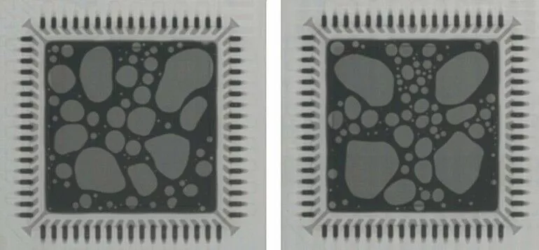
QFN voiding refers to the formation of air pockets or voids within solder joints during the assembly of Quad Flat No-lead (QFN) packages on printed circuit boards. These voids can compromise thermal performance, electrical conductivity, and overall reliability, leading to failures in high-stakes applications such as automotive electronics, consumer devices, and industrial controls. For engineers, technicians, and hobbyists searching for information on QFN voiding, this tag serves as a centralized resource to understand and mitigate these common assembly challenges. The content under this tag delves into the root causes of voiding, including factors like solder paste formulation, reflow profiles, and stencil design. Readers will find practical guidance on optimizing soldering processes to minimize voids, such as adjusting preheat times, using low-voiding pastes, or implementing vacuum reflow techniques. Best practices emphasize the importance of X-ray inspection for detecting voids post-assembly and design strategies like thermal pad patterning to enhance solder flow. By addressing these elements, users can improve yield rates and ensure long-term durability in their PCB projects. For those troubleshooting specific issues or seeking to refine their manufacturing workflows, the articles linked here offer in-depth case studies and step-by-step tutorials. Exploring these resources can provide the insights needed to tackle QFN voiding effectively, whether in prototype development or large-scale production. This collection aims to equip professionals with the knowledge to achieve void-free solder joints and elevate the quality of their electronic assemblies.
Video Guide
-
00:53
Technical Articles