










PCB Component Packages: QFP vs QFN vs BGA Tradeoffs Explained
What This Video Covers
This video reveals why the seemingly small decision of component PCB packages can determine the success or failure of your entire board — even with a perfect schematic. A package defines how a component connects to the PCB, how it is soldered during SMT assembly, and how well it withstands manufacturing and field stresses.
The video compares the most common types: QFP packages with exposed leads for easier visual inspection and rework. QFN packages that eliminate leads for superior electrical performance and thermal dissipation. BGA packages that hide connections underneath for maximum density and excellent high-speed signal integrity.
Each option brings tradeoffs. Smaller, finer-pitch packages increase risks of solder bridging, while hidden joints (especially BGAs) often require X-ray inspection. The right choice balances density, thermal management, reliability, and production yield.
Viewers gain practical guidance for real-world decisions during PCB prototype and PCB mass production. These considerations are vital for high-reliability applications including automotive PCB, medical devices PCB, and aerospace PCB, helping reduce costly revisions when ordering PCB assembly.
Key Highlights
- QFP packages offer exposed leads for straightforward inspection and rework, while QFN provides better thermal and electrical performance with no visible leads.
- BGA packages deliver the highest density and superior high-speed performance but hide solder joints, often requiring X-ray inspection after assembly.
- Package selection directly affects manufacturing risks, solder reliability, and overall board performance in dense or high-reliability designs.
Visual Comparison of QFP, QFN, and BGA Packages
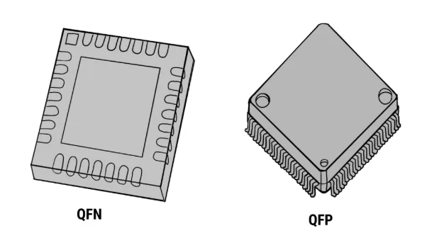
QFP packages feature gull-wing or J-lead configurations extending from the body, allowing direct visual access to solder joints. This design supports straightforward automated optical inspection (AOI) and manual rework with standard soldering tools. However, the extended leads increase the overall footprint, limiting use in ultra-dense layouts common in modern electronics.
QFN packages utilize a bottom-terminated design with a large central thermal pad and perimeter lands. The absence of protruding leads reduces parasitic inductance and improves signal integrity for higher-frequency applications. The exposed pad enhances heat transfer to the PCB, making QFN suitable for power management ICs and RF components where thermal dissipation is critical.
BGA packages arrange solder balls in a grid beneath the component, achieving the highest connection density. This configuration shortens trace lengths, minimizing signal degradation in high-speed digital interfaces such as DDR memory or processors. Production lines must implement controlled reflow profiles and void minimization strategies to ensure reliable ball-to-pad connections.
Manufacturing Challenges and DFM Considerations
In high-volume SMT assembly, QFP packages tolerate wider process windows for stencil printing and placement accuracy due to visible leads. However, fine-pitch QFPs (0.5 mm or less) are prone to solder bridging and lead deformation during handling or shipping. Design-for-manufacturing (DFM) guidelines recommend adequate clearance around leads and generous pad extensions to improve yield.
QFN packages demand precise stencil aperture design for the thermal pad to avoid solder starvation or excessive voiding. Insufficient paste volume on the center pad can lead to poor thermal contact and premature component failure under load. Manufacturers often specify via-in-pad designs with tented or filled vias to prevent solder wicking away from the joint.
BGA packages present the greatest inspection difficulties because solder joints are hidden. X-ray inspection becomes essential for detecting head-in-pillow defects, insufficient solder, or non-wet opens. DFM best practices include optimizing ball pitch, using appropriate via placement, and incorporating fiducials for accurate placement. In automotive and medical PCB production, additional process controls such as nitrogen reflow and strict moisture sensitivity level (MSL) handling are standard to mitigate risks.
Failure to address these package-specific challenges frequently results in field returns, particularly in vibration-prone or thermally cycled environments. Early collaboration between designers and manufacturers during the layout phase significantly reduces assembly defects and improves first-pass yield.
Comparison of QFP, QFN, and BGA Packages
| Package Type | Inspection Method | Thermal Performance | Density Level | Rework Difficulty | Typical Applications |
|---|---|---|---|---|---|
| QFP | AOI / Visual | Moderate | Medium | Low | General purpose, legacy designs |
| QFN | AOI + X-ray (limited) | Excellent | High | Medium | Power ICs, RF modules |
| BGA | X-ray required | Good to Excellent | Very High | High | Processors, high-speed memory, FPGAs |
Thermal and Electrical Performance Differences
Thermal management varies substantially across packages. QFN's large exposed pad provides a direct low-resistance thermal path to copper planes, often achieving lower junction temperatures compared to QFP in similar power dissipation scenarios. Proper copper pour and thermal via arrays are necessary to realize these benefits.
BGA packages distribute heat across many balls, enabling effective spreading when paired with appropriate PCB stack-up and heatsinking. However, in dense arrays, localized hot spots can develop if via placement or copper thickness is inadequate. Engineers must perform thermal simulations during design to validate performance under worst-case operating conditions.
Electrically, shorter interconnect paths in QFN and BGA reduce inductance and capacitance, supporting faster signal edges and lower crosstalk. QFP's longer leads introduce more parasitic effects, potentially requiring additional termination or layout compensation in high-speed designs. Signal integrity analysis tools should be used to quantify these differences before finalizing component selection.
Selection Guide for High-Reliability Applications
For automotive PCB and aerospace applications, reliability under thermal cycling and mechanical stress takes precedence. QFP remains viable where inspection access and reworkability are prioritized, such as in serviceable modules. QFN offers a strong balance for power electronics where heat dissipation and compact size are required. BGA is preferred for complex digital systems demanding maximum I/O count and superior signal performance, provided robust inspection and qualification processes are in place.
Medical devices PCB often combine multiple package types on a single board. Designers should evaluate component MSL ratings, CTE mismatch with the PCB substrate, and long-term reliability data from manufacturers. Prototype builds with accelerated life testing help validate package choices before committing to mass production.
FAQ
Q1: What are the main differences between QFP, QFN, and BGA packages?
A1: QFP has exposed leads for easy inspection, QFN removes leads for better thermal/electrical performance, and BGA hides balls underneath for highest density and high-speed applications.
Q2: Why do BGA packages increase manufacturing challenges?
A2: BGA packages hide solder joints, making them difficult to inspect visually and often requiring X-ray, while fine pitch increases risks of bridging and defects.
Q3: When should engineers prefer QFN over QFP packages?
A3: Choose QFN when better thermal dissipation and electrical performance are needed in space-constrained designs, accepting slightly harder rework compared to QFP.
Q4: How does package choice affect PCB assembly yield in volume production?
A4: Proper package selection aligned with DFM principles significantly improves first-pass yield. QFP generally offers higher visual inspection success rates, while QFN and BGA require tighter process controls and advanced inspection to maintain yields above 98% in high-reliability manufacturing.
Q5: What DFM steps minimize risks when using BGA components?
A5: Optimize pad design with non-solder mask defined (NSMD) pads, incorporate adequate thermal relief vias, follow recommended reflow profiles, and implement X-ray inspection protocols. Collaboration with the PCB assembly partner during the design review phase prevents common defects such as voiding or misalignment.
A PCB can fail...
even when the schematic is perfect.
So where does it go wrong?
Often, it's the package.
A PCB package is not just a chip shape.
It defines how the component connects, how it is soldered, and how it survives manufacturing.
Now the differences matter.
QFP packages expose their leads,
easier inspection and rework.
QFN packages remove leads,
better electrical performance and thermal behavior.
BGA packages hide everything underneath,
highest density, best for high-speed designs.
But here's the tradeoff.
Smaller packages increase manufacturing risk.
Fine pitch causes solder bridging.
Hidden joints are harder to inspect.
Some BGAs require X-ray after assembly.
So package choice is never mechanical.
It directly controls reliability, density, and manufacturability.





