










SMD Component Installation: Precision SMT Assembly for High-Reliability PCBs
What This Video Covers
This video demonstrates the complete SMD component installation process during SMT assembly, showing how modern equipment places and solders surface-mount devices onto PCBs with high precision. It covers key steps including solder paste application, component placement, reflow soldering, and post-assembly inspection to ensure strong mechanical and electrical connections.
The content is particularly useful for engineering and procurement teams who need consistent quality when scaling from prototype to mass production. It highlights practical techniques that reduce defects and improve long-term reliability in demanding applications such as automotive electronics, medical devices, and industrial control systems.
For a fast quote on your next SMD assembly project, use our PCB assembly quote (Instant PCB Assembly Quote & Calculator) tool or explore full PCB assembly capabilities.
Key Highlights
- Precise SMD component placement and reflow soldering for high-yield SMT assembly
- Quality inspection techniques that ensure reliable electrical and mechanical connections
- Scalable installation methods suitable for automotive, medical, and industrial PCB applications
The Complete SMD Component Installation Process in SMT Lines
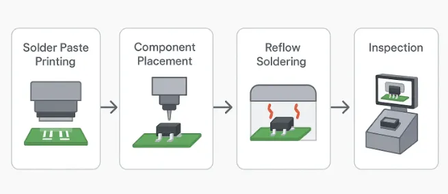
The SMD component installation sequence begins with precise solder paste deposition using laser-cut or electroformed stencils. Paste volume, aperture design, and print pressure must align with component footprint and PCB pad geometry to avoid insufficient or excess solder. Modern printers with automated inspection close the loop before components reach the board.
High-speed pick-and-place machines then position components using vision alignment systems. For fine-pitch and ultra-miniature packages (01005, 0201), placement force, nozzle selection, and feeder calibration directly impact first-pass yield. The process continues with controlled reflow soldering in multi-zone convection ovens, where the thermal profile follows a carefully ramp-soak-spike-cool sequence to achieve proper intermetallic formation without damaging components or the board.
Post-reflow, the assembly undergoes automated optical and X-ray inspection before moving to functional testing. Each step interlinks through process controls that maintain traceability and statistical process control (SPC) in high-volume environments.
Critical DFM Considerations for Successful SMD Placement
Design for manufacturability (DFM) for SMD component installation requires adequate pad-to-pad spacing, proper via placement, and thermal relief considerations around large components. Component orientation and polarity markings should support high-speed automated placement while allowing clear post-reflow inspection access.
Panelization and fiducial placement influence placement accuracy across the entire production panel. Designers should follow manufacturer-recommended land patterns and avoid placing tall components near fine-pitch devices that could create shadowing during reflow. Component selection also matters—standardized packages with good coplanarity reduce placement and soldering risks.
In practice, early collaboration between design and manufacturing teams catches issues such as insufficient solder mask clearance or mismatched thermal mass that could lead to defects in volume production.
SMD Package Type Comparison
| SMD Package Type | Typical Size | Placement Accuracy Requirement | Common Applications | Key DFM Note |
|---|---|---|---|---|
| 01005 / 0201 | 0.4×0.2 mm | ±25 µm | High-density wearables, medical | Extremely sensitive to paste volume |
| QFN / DFN | 2–6 mm | ±30–50 µm | Power management, RF | Hidden joints require X-ray |
| Fine-pitch QFP | 0.4–0.5 mm pitch | ±35 µm | Microcontrollers | Lead coplanarity critical |
| 0402 / 0603 | Standard | ±50 µm | General purpose | Most forgiving for prototypes |
Common Manufacturing Challenges and Defect Prevention Strategies
Tombstoning, solder bridging, and insufficient fillet formation remain frequent issues in SMD component installation. These often stem from uneven heating due to thermal mass differences, incorrect paste volume, or placement offsets. Optimized reflow profiles and nitrogen atmospheres help mitigate oxidation-related defects in lead-free processes.
Component floating or skewing during reflow can result from excessive paste or poor pad design. Manufacturers address this through precise stencil aperture adjustments, fiducial-based alignment verification, and real-time process monitoring. For high-reliability applications, additional measures include selective soldering validation and strict moisture sensitivity level (MSL) handling.
Practical recommendations include performing design rule checks (DRC) focused on SMT capabilities and running pilot runs with cross-section analysis to validate joint integrity before full production.
Advanced Inspection and Quality Control After SMD Installation
Post-installation verification combines 3D AOI for visible joint quality, X-ray for hidden connections under BGAs and QFNs, and electrical testing. These layered inspections catch defects that visual checks alone would miss, such as head-in-pillow or voiding in solder joints.
Statistical data from inspection systems feeds back into process adjustments, enabling continuous improvement in placement accuracy and reflow consistency. For critical applications, additional burn-in or environmental stress screening validates long-term performance under operating conditions.
Effective quality control integrates these methods into a closed-loop system that correlates defects with upstream parameters, reducing scrap and enhancing overall manufacturing efficiency.
Applications and Benefits Across Demanding Industries
SMD component installation techniques demonstrated in the video directly support high-reliability sectors. Automotive electronics require robust joints that withstand vibration and temperature cycling, while medical devices demand zero-defect traceability. Industrial control systems benefit from the high-density layouts enabled by precise SMT processes.
The scalability of these methods allows smooth transition from low-volume prototypes to mass production without major redesigns. Benefits include higher assembly yields, reduced warranty returns, and faster time-to-market for complex electronic products.
FAQ
Q1: What are the most common defects during SMD component installation and how are they prevented?
A1: Common defects include tombstoning, solder bridging, and insufficient solder joints. AIVON prevents these through precise stencil design, optimized solder paste volume, high-accuracy placement programming, and carefully controlled reflow profiles.
Q2: How does AIVON ensure placement accuracy for fine-pitch SMD components in high-volume production?
A2: AIVON uses high-speed SMT placement machines with 01005 and 0201 capability, real-time vision alignment systems, and closed-loop process control to maintain ±25 µm placement accuracy even during continuous high-volume runs.
Q3: Which inspection methods are used after SMD installation to verify solder joint quality?
A3: AIVON performs 3D Automated Optical Inspection (AOI), X-ray inspection for hidden joints, and in-circuit testing (ICT) after reflow soldering to ensure every SMD component meets strict quality standards.
Q4: What DFM changes most improve SMD component installation yield?
A4: Key improvements include using manufacturer-recommended land patterns, ensuring adequate clearance around fine-pitch devices, balancing thermal mass across the board, and incorporating proper fiducials. Early manufacturing input during layout significantly reduces defects in volume production.
Q5: How do reflow profiles affect SMD reliability in automotive and medical applications?
A5: Optimized profiles achieve proper wetting and intermetallic formation while staying within component temperature limits. In harsh environments, this prevents weak joints prone to cracking under thermal cycling or vibration, directly impacting product lifespan and safety compliance.
Today, we are installing a SMD IC onto the green PCB. First, align the component precisely with the solder pads. Using a fine-tip soldering iron and tweezers, carefully tack the corner pins to hold the IC in position.
Then, apply controlled heat and solder to each pin, ensuring clean joints without bridging. Pay close attention to temperature control to avoid damaging the component or lifting pads.
After soldering, inspect for cold joints or shorts. Clean any residue with isopropyl alcohol for a professional finish.
This technique is essential for reliable SMD assembly and repair.





