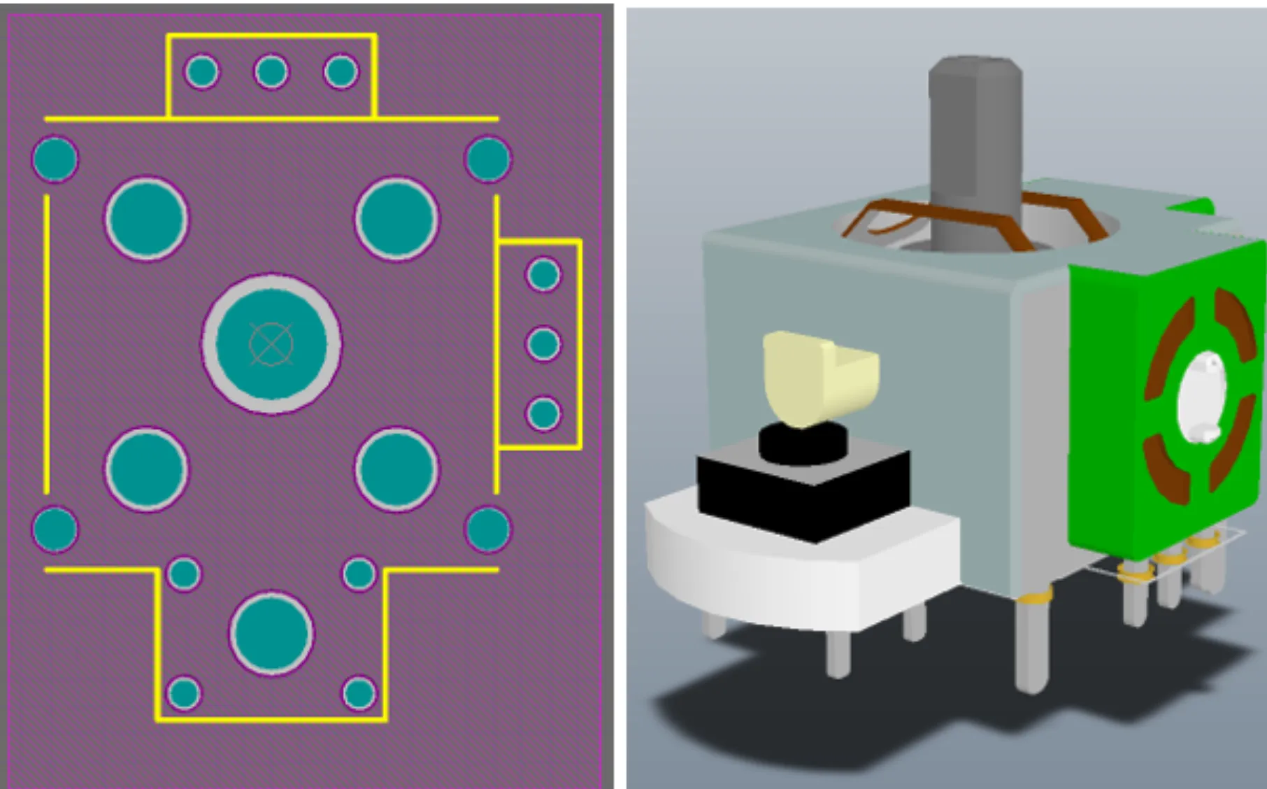
Solder Joint Design
Solder joint design plays a critical role in the reliability and performance of printed circuit boards (PCBs) and electronic assemblies. This tag encompasses a range of topics focused on optimizing the connections between components and PCBs through effective soldering techniques. Whether you are an electronics engineer troubleshooting assembly issues or a designer aiming to enhance product durability, understanding solder joint design helps prevent common failures such as cracks, voids, or thermal fatigue that can compromise device functionality. Key aspects covered include the selection of appropriate solder alloys, pad geometries, and reflow profiles to ensure strong mechanical and electrical bonds. For instance, incorporating rounded pad shapes and adequate spacing can minimize stress concentrations, while proper thermal management during soldering reduces the risk of intermetallic compound formation that leads to brittleness. Practical applications extend to high-reliability sectors like aerospace and automotive electronics, where robust solder joints are essential for withstanding vibration, temperature cycling, and environmental stresses. Best practices also emphasize inspection methods, such as X-ray analysis or shear testing, to verify joint integrity early in the production process. By delving into the articles under this tag, you can gain actionable insights into designing solder joints that meet industry standards like IPC-610, ultimately improving yield rates and extending product lifespan. These resources offer detailed guides on emerging trends, including lead-free soldering and advanced materials, equipping you with the knowledge to tackle real-world challenges in PCB manufacturing.
Technical Articles
Get in Touch
Send Message
- Products & Service
- Company
- About AIVON
- Contact
- News
- Blog
- Certification
-


- Payment
-


2026 AIVON.COM All Rights Reserved