










Fix Blocked Through-Hole on PCB After Soldering: Reliable Clearing Methods
What This Video Covers
This video addresses a common PCB soldering issue: through-holes blocked by excess solder, preventing component pins from inserting properly. It presents two practical fixes that restore clean, open holes without damaging the board.
The first method uses a dedicated desoldering tool for fast, repeatable results — simply heat and trigger to suction out the solder. The second manual approach employs a soldering iron and solder sucker: reheat the joint, add fresh solder to improve flow, then extract while fully molten. Timing and controlled heat are critical for clean results.
These techniques help maintain manufacturing flow during PCB prototype troubleshooting and PCB assembly rework. Proper hole clearing prevents assembly delays and supports reliable connections in multilayer and through-hole designs.
The guidance is valuable for high-reliability applications such as automotive PCB, industrial control PCB, and medical devices PCB, where clean through-hole preparation directly impacts product quality and yield.
Key Highlights
- Use a desoldering tool for fast, clean removal of excess solder from blocked through-holes.
- Manually clear holes with a soldering iron and solder sucker by reheating, adding fresh solder, and suctioning while molten.
- Proper technique leaves open, undamaged holes ready for component insertion without risking pad or trace issues.
Root Causes of Solder-Clogged Through-Holes in Assembly
Solder blockage occurs when the volume of alloy deposited exceeds the free space inside the plated barrel. Common contributing factors include oversized solder wire diameter relative to hole size, prolonged contact of the soldering iron tip that increases capillary flow, insufficient flux activity that allows the solder to solidify mid-flow, and incorrect wave-solder dwell or conveyor speed that leaves excess alloy inside the hole. In multilayer boards the thermal mass of internal planes further slows cooling, giving additional time for solder to fill the barrel completely.
From a DFM standpoint, hole-to-lead clearance that is already at the minimum IPC recommendation leaves little margin for process variation. When designers specify 0.2 mm annular rings or tight finished-hole diameters without accounting for plating thickness tolerance, even normal soldering variation can produce complete blockage. Recognition of these root causes allows process engineers to adjust solder volume, tip geometry, or flux chemistry before the defect becomes chronic.
Desoldering Tool Approach for Rapid and Controlled Removal
A dedicated desoldering station combines a heated hollow tip with an internal vacuum pump. The tip is placed squarely over the blocked hole, heat is applied until the solder becomes fully molten (typically 1–2 seconds at 350–370 °C for common Sn63/Pb37 or SAC305 alloys), and the vacuum trigger is activated. The molten alloy is drawn cleanly into the collection chamber, leaving the barrel walls free of residual solder.
Because heat and vacuum act simultaneously, the thermal excursion is short and localized. This reduces the risk of pad lifting on thin outer copper or of barrel cracking in high-aspect-ratio holes. In production rework cells the same tool can clear dozens of holes per hour with consistent results, making it the preferred method when throughput and repeatability are required. After each extraction the tip must be cleaned of residual alloy to maintain vacuum efficiency and prevent cross-contamination of subsequent joints.
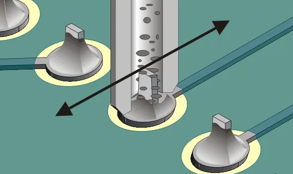
Manual Soldering Iron Combined with Solder Sucker Technique
When a desoldering station is unavailable, a standard soldering iron and spring-loaded solder sucker can achieve equivalent results. The sequence begins by reheating the blocked joint while adding a small amount of fresh solder and flux. The added alloy lowers the melting point of the existing mass and improves wetting, allowing the entire volume to become uniformly liquid. Once the solder is fully molten, the solder sucker nozzle is positioned directly over the hole and the vacuum is released in a single, firm stroke.
Timing is critical: extraction must occur while the alloy remains liquid. Premature actuation leaves partial blockage; delayed actuation allows the solder to begin solidifying on the barrel wall. After successful removal, a quick visual inspection under magnification confirms that no solder bridges remain between the pad and the hole wall. This manual method is particularly useful for field service or low-volume prototype laboratories where capital equipment is limited.
Comparison of Hole Clearing Methods
| Method | Primary Tools | Typical Cycle Time | Thermal Stress Level | Recommended Application |
|---|---|---|---|---|
| Desoldering Tool | Heated vacuum tip station | 2–4 s per hole | Low (simultaneous heat + vacuum) | High-volume rework, multilayer boards |
| Iron + Solder Sucker | Soldering iron, flux, solder sucker | 5–8 s per hole | Moderate (sequential heat then vacuum) | Prototype labs, field repair, limited tooling |
Thermal and Mechanical Risks During Hole Clearing
Excessive tip temperature or prolonged dwell can lift the annular ring, especially on boards with thin copper or large thermal reliefs. Rapid cooling after incomplete extraction may leave micro-voids or intermetallic layers that later cause intermittent opens under thermal cycling. Mechanical pressure from an improperly aligned solder-sucker nozzle can also deform soft copper pads or crack the barrel plating in high-aspect-ratio holes.
These failure modes are avoided by matching tip diameter to pad size, limiting contact time to the minimum required for full liquefaction, and verifying that the board is adequately supported to prevent flexure. In high-reliability sectors such as automotive, industrial control, and medical device PCBs, any residual damage discovered after clearing typically results in board scrap rather than attempted further repair, underscoring the value of first-time-correct technique.
Post-Clearing Verification and DFM Recommendations for Production
After the hole is cleared, visual inspection under 10× magnification confirms that the barrel walls are free of solder residue and that the pad surface remains flat and fully adhered. A go/no-go pin gauge matching the component lead diameter provides a rapid functional check. For multilayer boards, continuity testing between the cleared hole and internal planes verifies that plating integrity has not been compromised.
From a DFM perspective, designers can reduce the incidence of blockage by specifying finished-hole diameters that maintain at least 0.15 mm radial clearance after maximum plating thickness, selecting solder-mask-defined pads only when necessary, and documenting maximum allowable solder volume for each through-hole component. Process engineers further mitigate risk by locking wave-solder parameters, using nitrogen atmospheres to improve wetting control, and training operators on the exact heat-and-extract sequence demonstrated in the video. These combined measures keep assembly yield high and eliminate the need for repeated rework cycles.
FAQ
Q1: How do you clear a solder-blocked through-hole on a PCB?
A1: Heat the joint and use a desoldering tool or a soldering iron combined with a solder sucker to remove the excess solder while it is fully molten.
Q2: What is the best way to unclog through-holes without specialized tools?
A2: Reheat the joint with a soldering iron, add a small amount of fresh solder to improve flow, then use a solder sucker to pull out the molten solder.
Q3: Why does excess solder block through-holes during PCB soldering?
A3: Too much solder or poor technique during through-hole soldering can completely fill the plated hole, preventing component pins from inserting properly.
Q4: Can repeated heating damage the through-hole plating?
A4: Yes. Multiple thermal cycles without adequate cooling intervals can cause barrel cracking or intermetallic growth that weakens the copper plating. Limiting each clearing attempt to a single, well-executed heat-and-extract cycle preserves plating integrity.
Q5: How should cleared holes be inspected before component insertion?
A5: Use 10× magnification to confirm clean barrel walls and flat pads, followed by a pin-gauge check matching the component lead diameter. Continuity testing to internal planes is recommended for multilayer boards to verify plating continuity.
Through-hole blocked by sodder?
Now your pin just won't go through.
Too much sodder and the hole is completely clogged.
Two quick ways to fix it.
Fix one, use a desoldering tool.
Heat it up, trigger, and clear the hole.
Fast, clean, and repeatable.
No desoldering tool? You can still fix it manually.
Use a soldering iron and a solder sucker.
Reheat the joint, add a bit of fresh solder, then pull it out.
Timing matters, pull while it is fully molten.
Both methods work, one is faster, one is more flexible.
End goal, a clean open hole.





