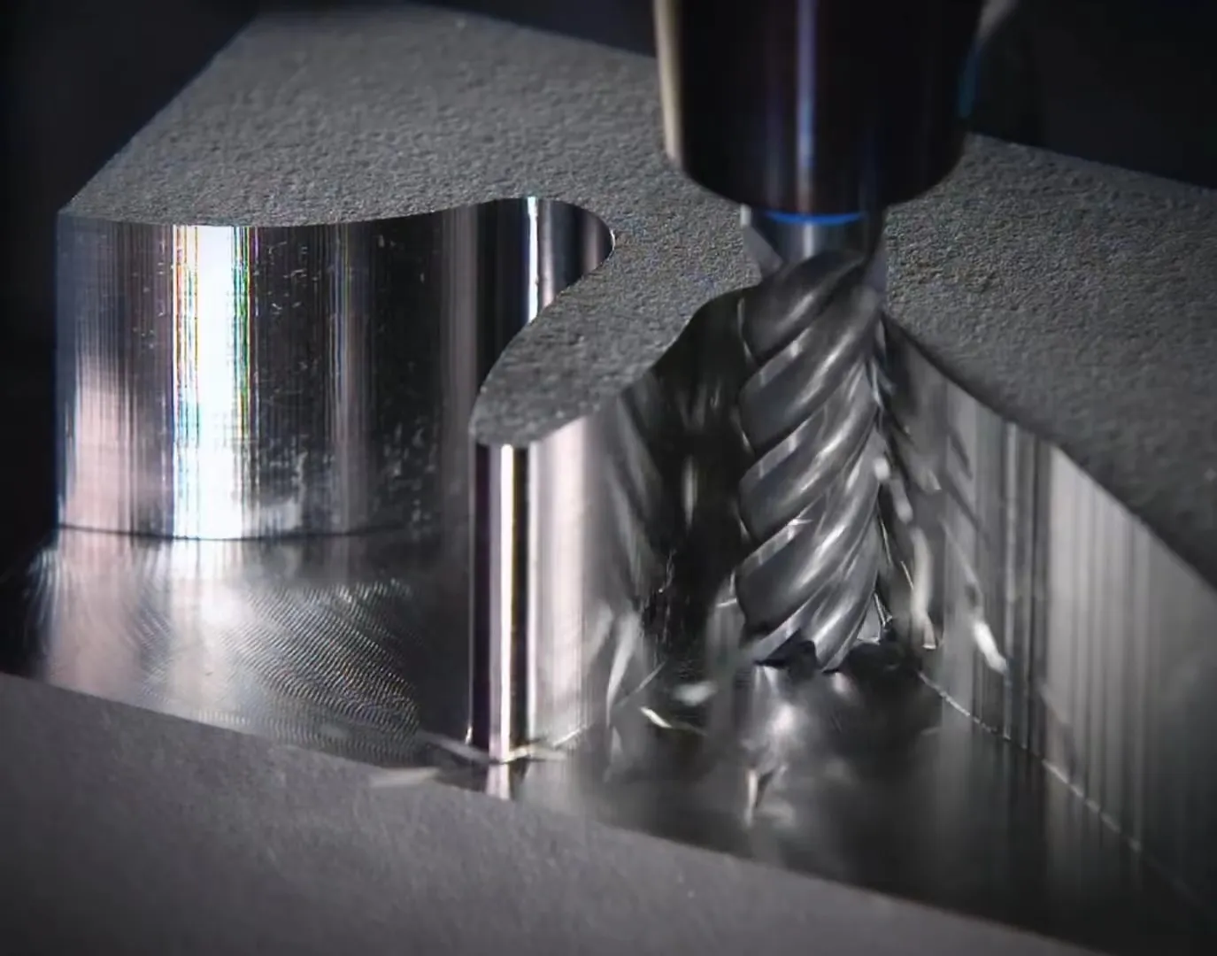
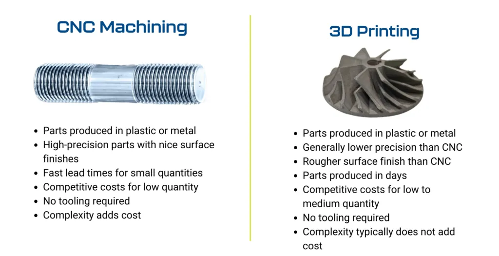
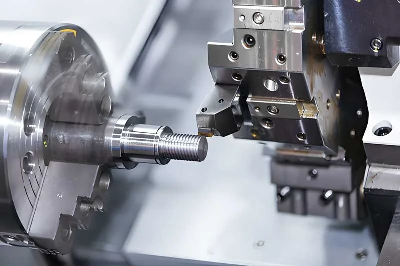
In production, we see CNC machined enclosures as the mechanical interface that has to line up with the PCB we just fabricated. CAM engineers start by pulling the enclosure STEP file alongside the board gerbers and drill files to verify fit before we commit to panelization or assembly prep. Most factories run a quick interference check and set standard clearances of 0.5 mm minimum between board edges and enclosure walls, adjusting mounting bosses to match our standard hole tolerances of ±0.1 mm.
What we typically see on the CAM side is that designers send enclosure files with wall thicknesses dipping below 2 mm in aluminum or inconsistent ribbing that causes vibration during our secondary machining steps for custom cutouts. We flag these early because the enclosure has to survive the same handling as the boards through assembly.
Wall thickness constraints that show up during enclosure milling
From a fabrication standpoint, wall thickness becomes sensitive once the CNC tool starts removing material from aluminum 6061 or similar stock. Thin sections under 2 mm tend to flex under cutter pressure, especially in deeper pockets meant to clear tall components on the PCB. In production this usually shows up as dimensional variation on the inner walls where the PCB needs to sit flat.
We handle this by recommending 2.5–3 mm nominal walls for most enclosures under 150 mm in length. This gives enough stiffness so the part stays stable when we machine mounting features or cut connector openings that align with the board layout. Thinner walls force slower feed rates and more passes, which directly hits cycle time on the shop floor.
How uneven walls affect panel-level processing
When enclosures come in with varying thickness, our fixturing for secondary operations becomes tricky. The part rocks slightly during drilling of additional holes or routing for cable exits, leading to positional errors relative to the PCB mounting points we already verified in DFM review.
Recommended Figure: Side-by-side comparison of proper uniform 2.5 mm wall thickness versus thin 1.2 mm section with deflection arrows during CNC tool path simulation.
Internal corner radii and tool access limitations in enclosure cavities
CNC cutters leave natural radii equal to their diameter, so sharp internal corners in the enclosure design force us to use very small tools or multiple setups. What we typically see is designers specifying 0.5 mm or smaller internal fillets when the pocket depth exceeds 3 times the tool diameter. This creates chatter marks and increases tool wear, especially around areas where the PCB edge or connectors will sit.
In the CNC PCB enclosure design guide context, we push for minimum internal radii of 1–1.5 mm matching common end mill sizes. This keeps the machining direction straightforward—usually starting from the open face of the enclosure—so the tool can clear the cavity without excessive tool changes.
Machining direction impact on feature accuracy
Most factories prefer to machine the enclosure from one primary direction to minimize setups. When mounting structures or ribs are oriented perpendicular to this access, we end up with additional fixturing steps that accumulate tolerance stack-up. This becomes noticeable when trying to align the PCB mounting holes precisely with pre-drilled board locations.
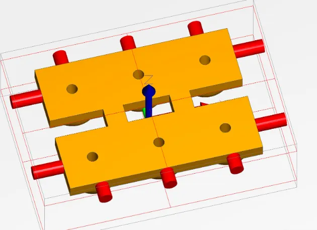
Production forces this limitation because each setup introduces minor rotational errors. We compensate by designing all critical PCB interface features—standoffs, card guides, and connector cutouts—on the same plane or accessible from the main cavity direction.
Mounting structure placement relative to PCB layout
On the CAM side, we check that enclosure bosses and threaded holes line up with the board’s mounting holes within ±0.15 mm. When designers place these structures too close to the enclosure walls—under 3–4 mm gap—we have to drop to smaller diameter tools, which slows production and risks breaking bits during deep pocketing.
We typically recommend standoff heights of 3–6 mm to clear common component heights on the PCB, with at least 0.5 mm clearance around the board perimeter for easy insertion and thermal expansion. This prevents binding during assembly that could stress the board or components.
Why tight mounting features cause downstream assembly issues
If mounting structures are not aligned with the PCB design, we see boards tilting during screw-down, leading to uneven pressure on connectors or potential trace damage near mounting holes. In our experience, this shows up more frequently in prototypes where the enclosure and board files were developed separately.
What happens when these guidelines are ignored in production flow
Thin walls or inadequate fillets tend to cause vibration during milling, resulting in surface finish issues and dimensional drift. This leads to enclosures that no longer fit the PCB snugly, forcing manual rework or scrap rates climbing in assembly batches. Misaligned mounting structures create cumulative tolerance problems—our drilled PCB holes no longer match the enclosure bosses, causing assembly delays or bent pins on connectors.
In one common case, deep narrow pockets without proper radii required extra setups, pushing lead times out by days and increasing tool consumption. Yield drops because the final assembly shows visible gaps or stress on the board when torqued down.
Factory-side adjustments and compensation methods for CNC enclosures
Most factories handle this by adjusting the CAM program to add generous fillets where possible and modifying tool paths for better access. We apply standard tolerances of ±0.1 mm on critical mounting features and use probing on the CNC to verify positions before full machining. Panel design strategies include leaving extra stock on enclosure blanks for secondary fixturing that maintains alignment with the PCB panel.
Process parameter control involves conservative feeds and speeds for thin sections, plus anodizing or other finishes applied after verifying fit with sample boards. Inspection uses coordinate measuring tools to check key dimensions against the PCB outline we received.
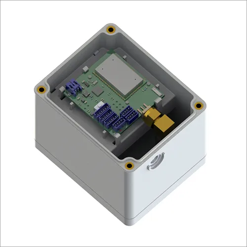
These methods are used because they reduce variability in the production flow where the PCB and enclosure come together late in the process. Early DFM review catches most issues before material is cut.
When we can relax enclosure tolerances in manufacturing
For low-volume prototypes or non-critical consumer devices, we sometimes allow wall thickness down to 1.8 mm if the overall size is small and no deep cavities are involved. Simple rectangular enclosures with minimal internal features can bypass some of the stricter machining direction rules by accepting additional setups, though this raises cost. Trade-offs include longer lead times and higher risk of minor cosmetic defects that do not affect PCB functionality.
High-volume runs or enclosures with IP rating requirements stay with the standard 2.5 mm+ walls and generous radii to keep yield high and assembly straightforward. Always share the full PCB mechanical drawing early so we can tailor the CNC programming accordingly.
This CNC PCB enclosure design guide approach keeps the mechanical and electrical sides aligned through production without constant back-and-forth on revisions. In practice, designs that follow these realities move through our lines with fewer holds and cleaner final assemblies.