PCB mounting hole design goes wrong fast when it doesn't match the realities of CNC-machined enclosures. I've reviewed hundreds of layouts where the holes sit a bit off, the tolerances stack up badly, or the screw size just doesn't fit the counterbore. The board either won't seat flat or it stresses the copper during assembly.
These issues show up most often because the mechanical CAD and PCB layout stay in separate worlds until the first prototype run. A few tenths of a millimeter matter here.
How Mounting Hole Position Creates Misalignment in CNC Enclosures
Engineers often place PCB mounting holes based on the enclosure drawing without accounting for the actual CNC machining tolerances. CNC enclosures typically hold ±0.1mm to ±0.2mm on hole positions depending on the shop and material. Yet many PCB layouts treat those coordinates as exact.
When the board gets screwed down, one or two holes bind while others sit loose. The PCB bows slightly. That bow creates micro-cracks in vias near the holes or lifts pads over time. In vibration environments it gets worse.
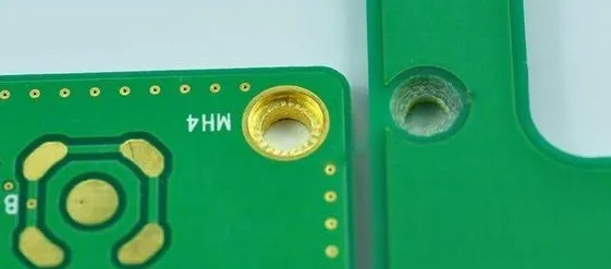
The common design choice is copying the enclosure hole pattern directly into the PCB footprint library. It looks perfect on paper. Reality hits when the enclosure vendor uses a different datum or the panel is fixtured differently during machining.
Tolerance Stack-Up Between PCB and CNC Enclosure Holes
PCB fabrication tolerances on mounting holes run around ±0.05mm to ±0.1mm for drilled holes, but the real problem is the cumulative error. Add enclosure tolerance, assembly fixturing, and thermal expansion. Aluminum enclosures expand more than FR-4 in the same temperature range.
I've seen boards where the holes were designed at nominal and ended up requiring force to align during final assembly. That force transfers directly to the solder joints on nearby components.
Better approach: design the PCB holes with slotted holes in at least one axis or oversize them appropriately. But oversizing has limits too.
Why Engineers Default to Tight Hole Positions
During layout it feels right to make everything match the 3D model exactly. Time pressure doesn't help. You want the board locked down solidly so it doesn't rattle. The instinct is good, but the execution ignores manufacturing variation.
CNC shops can hit tighter tolerances with extra setups and cost, but most cost-sensitive projects don't pay for that. The PCB mounting hole design has to accommodate standard capability.
Screw Size Selection and Its Effect on PCB Mounting Hole Design
M2.5, M3, #4-40 — the screw diameter drives everything. Too small a hole and the screw threads bind or the head sits crooked. Too large and the board has play, especially under shock.
Common failure: using the tap drill size instead of clearance size for the PCB hole. The screw needs to pass through freely while the enclosure thread holds it. Clearance holes should be screw diameter + 0.2mm to 0.4mm depending on length and expected misalignment.
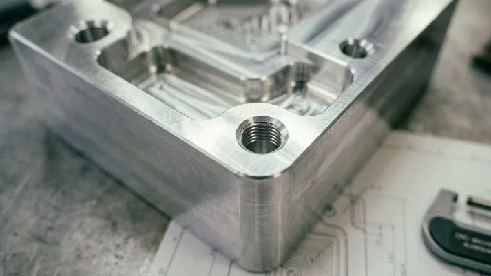
Counterbores add another layer. If the counterbore depth in the enclosure doesn't match the screw head height plus washer, the PCB won't sit flat. Boards have come back with lifted mounting pads because the screw bottomed out before clamping the board.
Positioning Challenges with Locating Features
Some designs rely on mounting holes for both mechanical fastening and alignment. That's risky. Better to have dedicated locating pins or asymmetrical features if polarization matters.
In CNC enclosures, the mounting bosses are often machined in the same operation as the outer walls. Any deviation in the enclosure outer dimensions shifts the relative hole positions. The PCB mounting hole design must include enough clearance or use floating fasteners.
Thermal cycling makes this worse. Different CTEs between the board, screws, and enclosure cause creep over time. Stainless screws in aluminum enclosures can loosen or over-stress the PCB laminate.
Practical Clearance Guidelines That Work in Production
For standard M3 screws I recommend 3.2mm to 3.6mm clearance holes in the PCB. Keep at least 0.5mm annular ring if the holes are plated. Non-plated holes can be smaller but watch for drill wander.
Distance from hole center to board edge should respect the enclosure wall thickness plus any draft angles. Keep copper at least 1.5mm away from the hole edge to avoid shorts if the screw head contacts the board.
In high vibration applications, consider captive screws or additional adhesive staking after assembly. But that's downstream — the layout still needs to start with realistic hole sizing.
Risks During Fabrication, Assembly, and Field Use
Bad PCB mounting hole design shows up first in assembly. Boards crack at the holes during torque-up. Or they sit proud and components on the bottom side get crushed against the enclosure.
In fabrication, tight tolerances on hole positions can cause panelization issues or drill breakage if the holes sit too close to other features. CAM engineers flag these when the design violates minimum web widths.
Long term, intermittent contact or stress on the mounting area leads to via fatigue or trace cracking. Especially problematic near high current paths or sensitive analog sections.
Adjusting Layout Decisions for Reliable PCB Mounting Hole Design
Start by getting the latest enclosure STEP file from the mechanical team and verify the hole coordinates against the 2D drawing. Then add 0.15mm to 0.25mm extra clearance in the critical axis.
Use IPC-7351 guidelines for land patterns but adjust for mechanical hardware. Plated mounting holes need sufficient copper for strength — aim for 1mm minimum annular ring on outer layers.
Keep the area around mounting holes clear of components for at least 5mm. This gives room for screwdrivers during assembly and prevents damage to nearby parts. No traces running directly under screw heads either.
For dense boards, consider using press-fit or snap features in the enclosure instead of relying solely on screws. But when screws are required, the PCB mounting hole design must treat them as a mechanical interface first, electrical second.
Key Lessons from Production Feedback
The best layouts treat mounting holes as critical mechanical features rather than afterthoughts. Coordinate early with the enclosure designer. Build in margin for real-world tolerances instead of hoping the shop hits perfect numbers.
Review the Gerber drill file against the enclosure drawing before release. Check hole sizes, positions, and plating callouts. A quick DFM review here saves far more time than fixing prototypes later.
Proper PCB mounting hole design doesn't add much layout time but prevents a lot of assembly headaches and field returns. The numbers are straightforward once you account for the full tolerance chain.
Next time you're laying out holes for a CNC enclosure, zoom out and think about the stack-up. Your future assembly team will thank you.