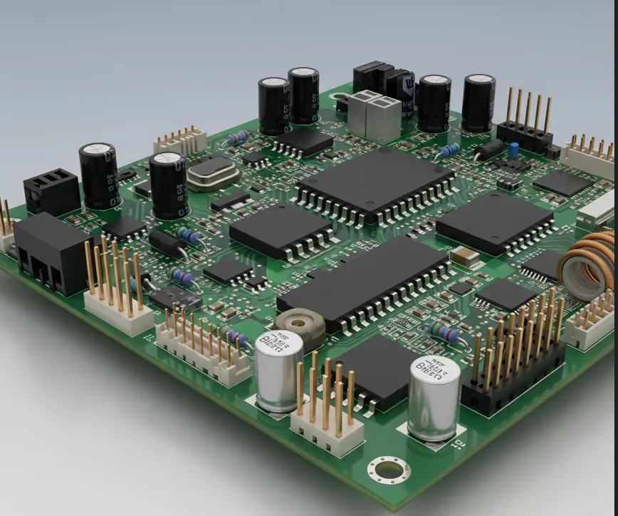
Poor component placement is one of the most common reasons a PCB design fails in routing, signal integrity, thermal performance, or manufacturing. Engineers often spend hours fixing crossed nets, long traces, or assembly issues that could have been avoided by treating placement as a deliberate engineering step rather than a quick drag-and-drop task.
In KiCad, component placement sets the foundation for everything that follows: Design Rule Check (DRC), routing, Gerber and drill file generation, BOM and pick-and-place export, DFM review, fabrication, and assembly. Good placement improves reliability, shortens design time, and reduces manufacturing risk. This article covers practical PCB layout principles and KiCad component placement methods that help you achieve both solid electrical performance and production-ready boards.
Why Component Placement Determines PCB Performance
Component placement directly controls signal path length, return current paths, thermal distribution, mechanical stress, and assembly yield. A poorly placed high-speed IC can force long, noisy traces. Heat-generating parts clustered together create hot spots. Components placed too close for the chosen assembly process cause soldering defects or inspection failures.
In the KiCad workflow, placement decisions are checked by DRC, influence how cleanly you can route, and ultimately appear in the manufacturing package (Gerbers, drill files, centroid data). Manufacturers evaluate placement density, orientation consistency, and clearances during DFM review. Fixing placement problems after routing or after receiving boards is far more expensive than getting it right early.
Planning Component Placement Before Routing
Treat placement as a planning phase, not an afterthought. Before moving any footprints in the PCB Editor, review the schematic hierarchy, critical nets, power domains, and mechanical constraints.
Functional Grouping
Group components by function: power section, analog front-end, digital core, connectors, and interface circuits. Place related parts close together so that local routing stays short and power/ground loops remain tight.
In KiCad, use the schematic hierarchy and net labels to identify functional blocks. In the PCB Editor, select related footprints and move them as a group (or use rooms if you define them). This approach reduces crosstalk between analog and digital sections and makes later DRC cleaner.
Common mistake: scattering bypass capacitors far from IC power pins. Always place decoupling capacitors immediately adjacent to the pins they serve.
Signal Flow Consideration
Follow the natural signal path from input to output or from source to load. Place connectors and sensors near the board edge where signals enter or leave. Keep high-speed or sensitive paths short and direct.
Visualize the flow on paper or with a rough floorplan before detailed placement. In KiCad, use the Ratsnest (visible ratsnest lines) as a guide—minimize the length and crossing of major nets early.

Basic Placement Rules
These rules apply to almost every board and form the baseline for reliable manufacturing.
Component Orientation
Orient similar components in the same direction whenever possible. Align polarized parts (electrolytic capacitors, diodes, ICs with pin-1 markers) consistently. This simplifies visual inspection, automated optical inspection (AOI), and manual assembly.
In KiCad, use the "Rotate" and "Flip" tools carefully. Keep pin-1 indicators visible and consistent across the board. For dual-sided designs, decide early which side receives the majority of components to simplify the pick-and-place process.
Spacing Requirements
Maintain adequate clearance between components for routing channels, solder mask bridges, and reflow or wave soldering. Follow the manufacturer's recommended land pattern clearances and add extra margin for dense designs.
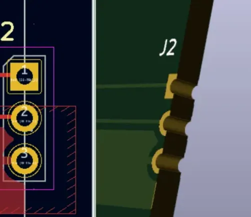
KiCad's Design Rules and DRC catch many spacing violations, but placement-time judgment is still required. Leave room for vias, thermal reliefs, and probe points. Avoid placing tall components next to low-profile ones in ways that block airflow or inspection.
Assembly Considerations
Think about how the board will be assembled. Keep components at least a minimum distance from board edges for panelization and handling. Orient connectors so that cables exit cleanly. Place test points and fiducials where they remain accessible.
Polarized and fine-pitch parts benefit from consistent orientation because it reduces placement machine errors and visual mistakes. After placement, run DRC and review the 3D viewer in KiCad to catch height conflicts early.
High-Speed Component Placement Guidelines
High-speed sections require stricter placement discipline because every extra millimeter of trace length or poor return path degrades signal integrity.
Processor Placement
Place the processor (MCU, FPGA, or SoC) near the center or in a location that allows short paths to memory, clocks, and critical interfaces. Keep the crystal or oscillator very close to the processor pins with a solid ground plane underneath. Route power and ground first in that local area.
Avoid placing the processor near noisy switching regulators or high-current paths.
Memory Placement
Position memory devices (DDR, Flash, SRAM) immediately adjacent to the processor with matched-length considerations already in mind. Keep address, data, and control buses short and parallel where possible. Place termination resistors and decoupling close to the memory package.
Differential Signal Considerations
For differential pairs (USB, Ethernet, PCIe, LVDS), place the transmitter and receiver pairs so that the differential traces can run with controlled impedance and minimal length difference. Keep the pair together from the start of placement. Avoid placing noisy components or discontinuous reference planes under differential routes.
In KiCad, after placement, use the Interactive Router with differential pair mode and length-tuning tools. Early placement decisions determine how easily these tools can meet timing requirements.
Thermal and Mechanical Considerations
Heat-Generating Components
Identify power regulators, drivers, processors, and power resistors that dissipate significant heat. Place them with adequate copper area for heat spreading, away from temperature-sensitive parts (precision references, sensors, batteries). Provide thermal vias under exposed pads when the footprint requires them.
In KiCad, review the footprint's thermal pad and copper requirements. Use the 3D viewer and, if available, thermal simulation data to validate placement. Cluster heat sources only when the board has intentional heat-spreading features or a heatsink plan.
Mechanical Restrictions
Respect keep-out zones for mounting holes, connectors, shields, and enclosure features. Place tall components where they will not interfere with the mechanical assembly. Orient connectors according to cable routing in the final product.
Import the mechanical outline and keep-out layers into KiCad early so placement stays within real constraints. Violating mechanical limits often forces last-minute respins.

Manufacturing-Friendly Placement Tips
Placement that looks good electrically can still fail at the fab or assembly house. Focus on these practical points:
- Maintain consistent component orientation and polarity marking visibility.
- Provide sufficient clearance for solder paste stencils and reflow profiles.
- Place fiducials in standard locations and keep them clear of components and silkscreen.
- Avoid placing fine-pitch or BGA parts near board edges or in high-stress areas.
- Group similar package types when possible to simplify pick-and-place programming.
- Leave space for test points and debug headers without compromising critical routing.
After placement and routing, run a full DRC in KiCad, generate Gerbers, drill files, BOM, and pick-and-place (centroid) files. Review the manufacturing package for density issues, missing fiducials, or orientation inconsistencies. A clean package reduces DFM queries and speeds up production.
After completing the KiCad design process, engineers can export manufacturing files and submit them to AIVON for PCB fabrication and assembly. This closes the loop from placement decisions through to a manufacturable board.

FAQ
Q1: What is the best way to start component placement in KiCad?
A1: Begin with a floorplan based on functional grouping and signal flow. Place connectors and critical ICs first, then supporting passives. Use the ratsnest and schematic hierarchy as guides before detailed positioning.
Q2: How close should decoupling capacitors be placed to IC power pins in KiCad?
A2: Place them as close as the footprint and routing allow—ideally adjacent to the pins with short, wide traces or vias directly to the power plane. Long connections reduce the effectiveness of the capacitor.
Q3: Does component placement affect PCB manufacturing cost and yield?
A3: Yes. Consistent orientation, proper spacing, clear fiducials, and avoidance of edge crowding improve assembly yield and reduce DFM issues. Dense or poorly oriented layouts increase the chance of soldering defects and inspection failures.
Q4: How do I check placement quality before routing in KiCad?
A4: Run DRC with appropriate clearance and courtyard rules, inspect the 3D viewer for height and mechanical conflicts, and review ratsnest lengths for critical nets. Fix placement problems at this stage rather than after routing.
Q5: What placement rules help with high-speed and differential signals?
A5: Keep processors and memory close, place crystals next to the IC, and position differential pair sources and loads so that short, matched-length routes are possible. Maintain continuous reference planes under these sections from the start of placement.