Introduction
In demanding applications such as aerospace, medical devices, and automotive electronics, PCB assembly must achieve exceptional reliability to prevent failures that could have severe consequences. Electric engineers face constant pressure to optimize processes that enhance solder joint reliability while minimizing risks from thermal stresses and mechanical vibrations. PCB assembly best practices focus on precise control over every stage, from stencil printing to final inspection, ensuring components withstand harsh environments over extended lifecycles. Preventing assembly defects through meticulous planning and automated assembly techniques for high-reliability becomes essential for meeting performance targets. This article explores proven strategies tailored for engineers troubleshooting real-world challenges in high-stakes production. By integrating component placement for reliability with rigorous quality checks, assemblies can exceed standard expectations.
Why High-Reliability PCB Assembly Matters
High-reliability PCB assembly refers to processes designed for class 3 products under IPC-A-610J criteria, where electronics operate in uninterrupted critical service with no downtime allowed. These assemblies power systems in satellites, life-support equipment, and electric vehicles, where a single defect can lead to mission failure or safety hazards. Engineers prioritize solder joint reliability because fatigue from thermal cycling often causes the most common failures in these environments. Component placement for reliability directly influences stress distribution, preventing cracks at board edges or under large components. Without adherence to PCB assembly best practices, even minor variations in reflow profiles amplify defect rates, escalating costs during rework. Ultimately, investing in these techniques ensures compliance with industry demands for longevity and robustness.
Key Technical Principles Affecting Assembly Reliability
Solder joint reliability hinges on intermetallic compound formation during reflow, where inadequate control leads to brittle interfaces prone to cracking under vibration. Thermal expansion mismatches between components, solder, and the PCB substrate generate shear stresses, particularly in multilayer boards with fine-pitch devices. Component placement for reliability requires strategic orientation to minimize these mismatches, such as positioning heat-sensitive parts away from high-power sources. Warpage from uneven cooling exacerbates defects like head-in-pillow, where the solder ball fails to fully wet the pad. Moisture absorption prior to assembly can cause voids or delamination, underscoring the need for controlled storage conditions. Understanding these mechanisms allows engineers to predict and mitigate risks through process optimization.
Preventing assembly defects starts with material selection, as alloy choices impact melting points and wetting behavior without introducing excess oxides. Automated assembly techniques for high-reliability leverage vision systems to detect pad misalignment before placement, reducing tombstoning in chip components. Electrical testing post-reflow verifies continuity, but acoustic microscopy reveals hidden voids invisible to optical inspection. Engineers troubleshooting these issues often trace root causes to SMT stencil aperture design, where improper release of solder paste creates insufficient volume. Balancing paste viscosity and printing pressure proves critical for consistent deposits across varying pad sizes.
Best Practices for Solder Joint Reliability
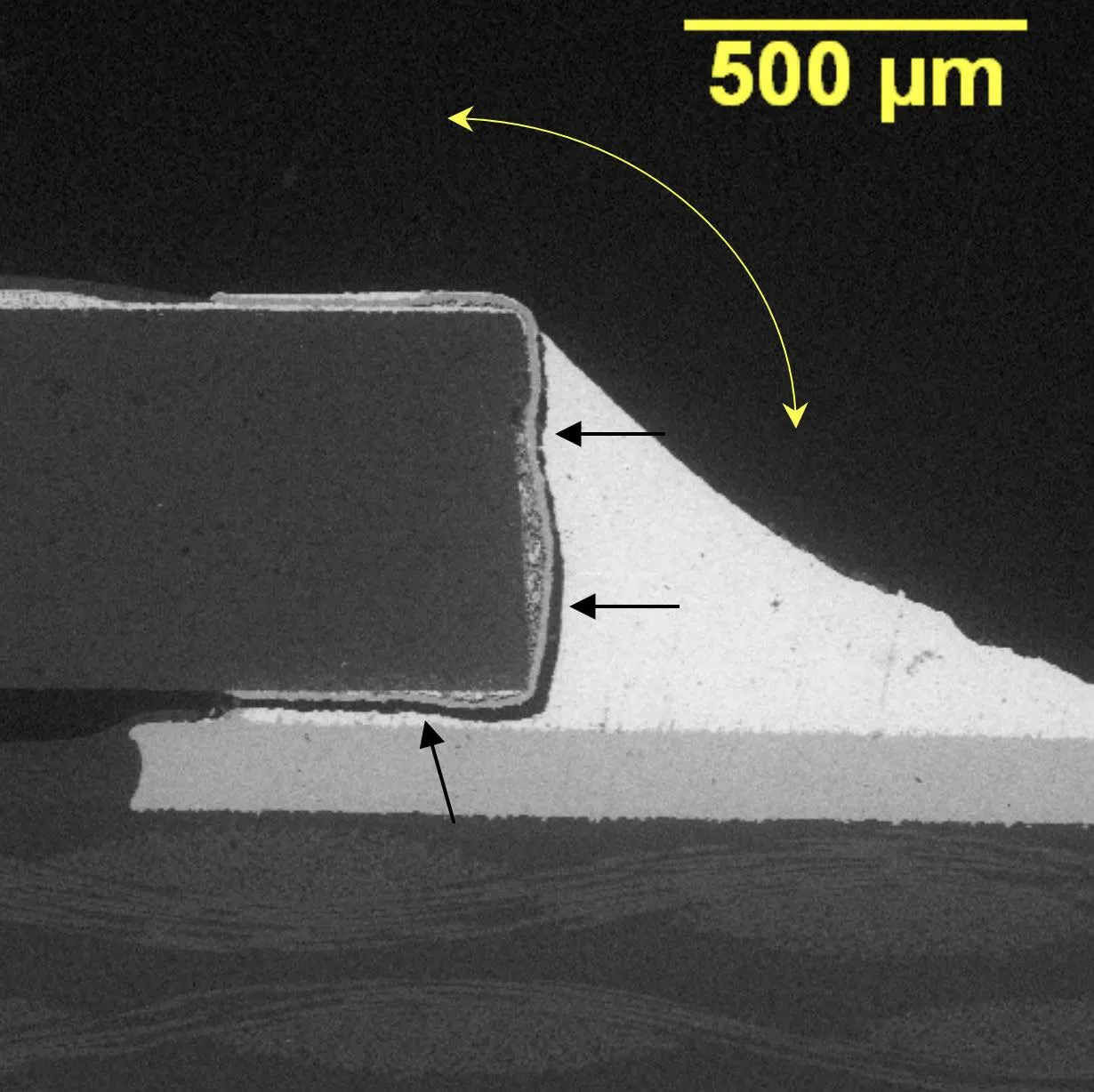
Implement stencil printing with laser-cut apertures sized 10-20% larger than pads to ensure optimal solder paste volume, directly boosting joint fillet formation. Engineers should validate reflow profiles using thermocouples on test boards, targeting peak temperatures that achieve full melt without overheating. Flux selection favors no-clean types with high activity to promote wetting on oxidized surfaces, minimizing bridges between closely spaced leads. Post-print inspection via SPI confirms uniform deposits, preventing defects that propagate through reflow. Adhering to J-STD-001J guidelines for soldering requirements ensures joints meet criteria for high-reliability applications, including void limits under 25% for BGAs. Regular profilometer checks on stencils maintain aperture integrity, avoiding paste starvation over production runs.
Cleaning processes post-reflow remove residues that could initiate dendritic growth under humidity, with ionic contamination testing quantifying risks. Nitrogen atmospheres during reflow reduce oxidation, enhancing intermetallic layer uniformity for better fatigue resistance. For lead-free alloys, extended preheat times allow gradual flux activation, preventing dewetting on copper pads. These PCB assembly best practices collectively extend joint life cycles by addressing fatigue precursors early.
Optimizing Component Placement for Reliability
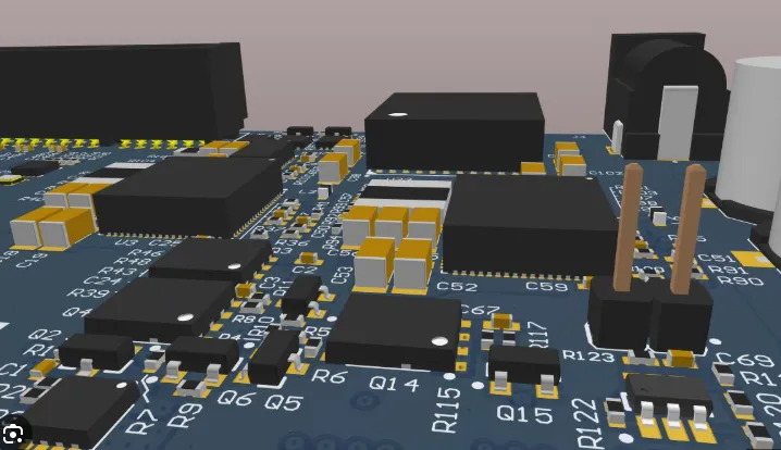
Strategic component placement for reliability begins with thermal modeling to identify hotspots, directing high-dissipation devices toward board centers with adequate airflow paths. Fine-pitch QFNs demand symmetric pad layouts to equalize solder joint stresses during board flexure. Engineers troubleshoot misalignment by calibrating pick-and-place nozzles for vacuum hold consistency, especially on warped panels. Spacing rules prevent shadowing during reflow, where taller components block heat from adjacent low-profile parts. Fiducial marks on panels guide automated systems precisely, reducing offsets below 50 microns for BGA arrays. Grouping analog and digital sections minimizes crosstalk while preserving mechanical stability. By integrating these high-performance PCB assembly key design considerations early in the process, engineering teams can ensure their layouts meet the rigorous manufacturing standards expected in the coming years.
Panelization techniques influence placement accuracy, as edge support rails prevent sagging in large arrays. For high-vibration environments, reinforcing vias near connectors anchors the assembly against cyclic loading. Post-placement verification with 3D AOI catches rotations or absences before reflow commits the board. These practices ensure uniform stress distribution, vital for long-term solder joint reliability.
Preventing Common Assembly Defects
Preventing assembly defects requires ESD-safe handling from incoming inspection through packaging, as static discharges pit component leads. Solder paste refrigeration at 4-10°C preserves tackiness, with room-temperature equilibration before printing to avoid condensation. Engineers often diagnose bridging via high-speed cameras during reflow, adjusting conveyor speeds for even heating. Tombstoning mitigation involves balanced pad sizes, where the larger ground pad anchors the component against surface tension pull. Warpage control uses low-CTE substrates matched to assembly processes, measured via shadow moiré post-lamination.
Incoming quality checks on reels reject bent leads or chipped ceramics, preempting placement failures. Automated optical inspection flags foreign object debris before reflow, where molten solder could encapsulate contaminants. Bake-out protocols desorb moisture from components per classification levels, preventing popcorning. These layered defenses form the core of PCB assembly best practices.
Automated Assembly Techniques for High-Reliability
Automated assembly techniques for high-reliability employ dual-lane feeders for continuous operation, minimizing downtime in high-volume runs. Vision-guided robotics handle odd-form components with force feedback, preventing pad damage on fragile boards. Jet printing replaces traditional stencils for variable paste volumes, ideal for mixed-technology panels. In-line X-ray systems inspect BGA voids non-destructively, feeding data back for real-time process tweaks. High-speed SPI integrates with placement machines, halting lines on defect trends.
Feeder calibration verifies tape advance accuracy, crucial for 01005 chips where tolerances approach 25 microns. Nitrogen-purged ovens maintain consistent reflow atmospheres across batches. Functional circuit testing post-assembly simulates operational stresses, weeding out latent defects. These techniques scale reliability without proportional cost increases.
Troubleshooting Insights for High-Reliability Assemblies
When solder balls lift during reflow, check for excessive ramp rates causing uneven melting, slowing preheat to stabilize. Head-in-pillow defects signal pad non-planarity, addressed by chemical planarization or selective soldering hybrids. Vibration-induced cracks post-assembly trace to inadequate underfill for large BGAs, applied via capillary flow with cure verification. Engineers log defect Pareto charts to prioritize stencil redesigns yielding the highest ROI. Cross-section analysis confirms IMC thickness, guiding alloy tweaks within process windows.
Conclusion
Mastering PCB assembly best practices elevates solder joint reliability, optimizes component placement for reliability, and curbs defects through proactive measures. Automated assembly techniques for high-reliability streamline production while upholding class 3 standards like IPC-A-610J. Electric engineers benefit from these strategies by reducing field failures and accelerating time-to-market. Consistent application across the process chain delivers assemblies ready for extreme conditions. Prioritize data-driven troubleshooting to refine operations continually.
FAQs
Q1: What are the key PCB assembly best practices for enhancing solder joint reliability?
A1: Focus on precise stencil printing, validated reflow profiles, and post-reflow cleanliness to minimize voids and cracks. Adhere to J-STD-001J for soldering criteria, ensuring full wetting and controlled intermetallics. Automated SPI and AOI catch inconsistencies early, while nitrogen reflow prevents oxidation. These steps directly improve fatigue life in high-stress environments. Regular process audits maintain consistency.
Q2: How does component placement for reliability impact overall PCB performance?
A2: Optimal placement reduces thermal gradients and mechanical stresses on solder joints by grouping heat sources strategically. Symmetric layouts for fine-pitch devices prevent warping-induced failures during operation. Vision systems ensure micron-level accuracy, avoiding reflow defects like tombstoning. Engineers model stress flows pre-layout for vibration-prone apps. This approach extends assembly lifespan significantly.
Q3: What techniques prevent assembly defects in high-reliability PCBs?
A3: ESD controls, moisture bake-out, and debris-free environments form the foundation. SPI verifies paste volume uniformity, while X-ray checks hidden BGA issues. Stencil maintenance avoids bridging, and balanced pad designs curb lifting. Troubleshooting Pareto analysis targets recurring problems efficiently. These prevent assembly defects proactively.
Q4: Why choose automated assembly techniques for high-reliability production?
A4: Automation delivers sub-50-micron placement precision and real-time defect feedback via integrated AOI/X-ray. Jet dispensers adapt to mixed pitches without stencil changes, boosting throughput. Force-monitored handling protects fragile parts, ensuring IPC-A-610J class 3 compliance. Data logging enables predictive maintenance, cutting variability. Ideal for scaling without reliability trade-offs.
References
IPC-A-610J — Acceptability of Electronic Assemblies. IPC, 2024
IPC J-STD-001J — Requirements for Soldered Electrical and Electronic Assemblies. IPC, 2024