Introduction
Stencil printing stands as a foundational process in modern PCB assembly, especially when working with lead-free solder paste. This technique directly influences the quality and reliability of soldered connections in electronic devices. As environmental regulations push the industry toward lead-free assembly, understanding the nuances of stencil printing becomes critical for engineers. Lead-free solder paste, while eco-friendly, presents unique challenges like higher melting points and different flow characteristics compared to traditional lead-based options. This article explores the best practices for stencil printing with lead-free solder paste to ensure consistent, defect-free results in PCB assembly. From material selection to process optimization, these insights aim to help electric engineers achieve reliable soldering outcomes while adhering to industry standards.
What Is Stencil Printing and Why It Matters in PCB Assembly
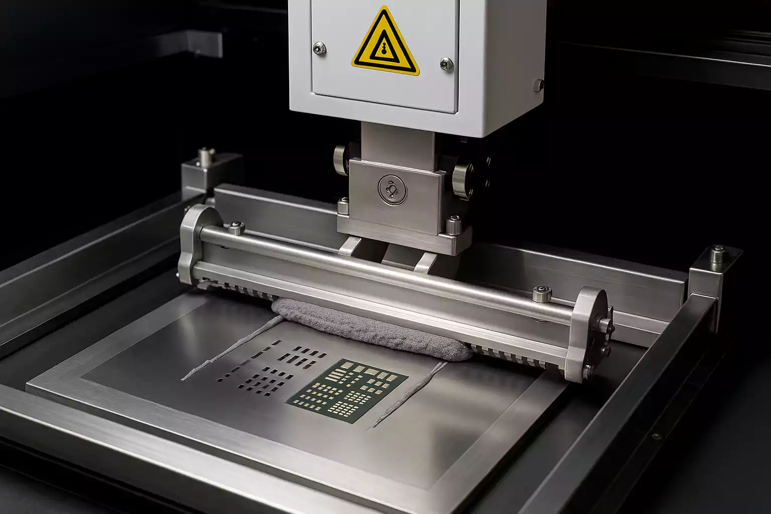
Stencil printing involves applying solder paste onto a printed circuit board through a thin metal stencil with precisely cut apertures. This process is vital in surface mount technology, where components are mounted directly onto the PCB surface. The accuracy of solder paste deposition determines the quality of solder joints, impacting electrical performance and mechanical stability. In lead-free assembly, the importance of stencil printing is amplified due to the unique properties of lead-free solder paste, such as reduced wettability and higher viscosity. Poor printing can lead to defects like insufficient solder, bridging, or tombstoning, all of which compromise assembly reliability. For engineers, mastering this step is essential to meet stringent quality requirements and ensure long-term functionality of electronic products.
Key Properties of Lead-Free Solder Pastes
Lead-free solder pastes are primarily SAC (tin-silver-copper) alloys blended with flux vehicles. Understanding their properties is essential for successful printing and reflow.
The table below compares popular alloys:
| Alloy | Melting Point (°C) | Typical Particle Size | Viscosity (Pa·s) | Flux Chemistry Options | Printability | Wettability | Best Applications | Relative Cost |
|---|---|---|---|---|---|---|---|---|
| SAC305 | 217–220 | Type 4–5 | 150–200 | No-clean or water-soluble | Good | Moderate | General SMT, consumer, industrial | Medium |
| SAC387 | 217–220 | Type 4–6 | 160–220 | No-clean | Fair | Lower | High-reliability, aerospace | Higher |
| SnBiAg (low-temp) | 138–170 | Type 5–6 | 120–180 | No-clean | Excellent | Good | Temperature-sensitive assemblies | Lower |
| SAC405 | 217–220 | Type 4 | 140–190 | Water-soluble | Very Good | Good | Fine-pitch, high-speed lines | Medium |
Table 1: Comparison of common lead-free solder paste alloys (2026 typical values). Data synthesized from major suppliers; always verify current datasheets.
Viscosity ranges from 150–220 Pa·s, significantly higher than tin-lead pastes, requiring adjusted printer settings. Particle size (Type 4 = 20–38 µm, Type 5 = 15–25 µm, Type 6 = 5–15 µm) affects both print definition and voiding risk—finer powders improve fine-pitch release but increase oxidation sensitivity. Flux chemistry determines activity, residue cleanliness, and compatibility with cleaning processes. Retaining the original insight on higher melting temperatures and flow characteristics, these properties demand tighter process windows than traditional materials to prevent defects during stencil printing with lead-free solder paste.
Technical Principles of Stencil Printing with Lead-Free Solder Paste
Understanding the technical aspects of stencil printing is key to achieving consistent results with lead-free solder paste. The process relies on several interconnected factors, including stencil design, paste composition, and equipment settings. Lead-free solder paste typically consists of tin, silver, and copper alloys, which have higher melting temperatures compared to traditional tin-lead compositions. This necessitates precise control over printing parameters to ensure proper paste transfer.
The stencil itself plays a critical role. Its thickness, aperture size, and shape must align with the PCB pad layout and component requirements. A common guideline, as outlined in widely recognized industry standards, is maintaining an appropriate aspect ratio and area ratio for apertures to facilitate clean paste release. The aspect ratio, defined as the aperture width divided by stencil thickness, should generally be above a specified threshold to prevent clogging. Similarly, the area ratio, which considers the aperture area relative to the stencil wall area, must meet minimum values for effective transfer.
Lead-free solder paste also exhibits higher viscosity, which can affect how it flows through stencil apertures. This property requires careful adjustment of printing speed and pressure to avoid defects like incomplete deposits or smearing. Temperature and humidity control in the assembly environment further influence paste behavior, as excessive moisture can alter its consistency. Engineers must account for these variables to maintain process stability during SMT PCB assembly.
Challenges Specific to Lead-Free Solder Paste in Stencil Printing
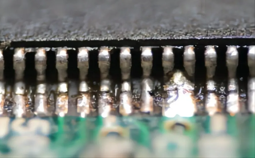
Lead-free solder paste introduces several challenges during stencil printing that differ from traditional solder materials. One primary issue is its reduced wettability, which can lead to poor adhesion to PCB pads and increased risk of defects like solder balling. The higher melting point of lead-free alloys also means that the paste may not spread as easily during printing, potentially causing uneven deposits. Additionally, the shelf life and storage requirements of lead-free paste are often stricter, as it can be more prone to oxidation over time.
Another challenge is the interaction between lead-free paste and stencil materials. The paste’s abrasive nature can accelerate stencil wear, especially with frequent use. This wear affects aperture precision, leading to inconsistent paste volumes. Engineers must monitor stencil condition and plan for regular maintenance to mitigate this issue. Understanding these challenges is the first step toward implementing effective soldering techniques tailored for lead-free assembly. Regular maintenance is critical; see our guide on optimizing solder paste stencil design for flawless PCB assembly for detailed aperture and material recommendations.
Best Practices for Reliable Stencil Printing with Lead-Free Solder Paste
Achieving reliable results in stencil printing with lead-free solder paste requires adherence to proven best practices. These guidelines, grounded in industry standards, help electric engineers optimize the process for consistent PCB assembly outcomes.
Stencil Design Optimization
Start with a well-designed stencil tailored to the specific requirements of lead-free solder paste. Ensure that aperture dimensions match the PCB pad sizes while maintaining recommended aspect and area ratios, as specified in standards like IPC-7525B, Stencil Design Guidelines. For fine-pitch components, consider using stepped stencils to vary thickness across different areas, providing better control over paste volume. Select stencil materials with high durability to withstand the abrasive nature of lead-free paste.
Solder Paste Selection and Handling
Choose a lead-free solder paste with properties suited to the assembly process. Factors like particle size and flux type impact printability and reflow performance. Store the paste under recommended conditions, typically in a refrigerated environment, to prevent oxidation and maintain consistency. Before use, allow the paste to reach room temperature gradually to avoid condensation, which can alter its viscosity. Always follow handling guidelines to ensure the paste remains within its usable shelf life.
Printing Process Parameters
Adjust printer settings to accommodate the unique characteristics of lead-free solder paste. Optimize squeegee pressure and speed to achieve uniform paste transfer without excessive force, which can damage the stencil or smear the paste. Maintain a consistent separation speed between the stencil and fast turn PCB to ensure clean release. Regularly inspect the underside of the stencil for residue buildup and clean it using appropriate solvents to prevent clogging.
Environmental Control
Control the assembly environment to minimize variables affecting lead-free solder paste. Maintain temperature and humidity within specified ranges to preserve paste consistency. Excessive humidity can cause the paste to absorb moisture, leading to printing defects. A controlled environment also reduces the risk of oxidation on PCB pads, improving solder joint quality during reflow.
Inspection and Maintenance
Implement routine inspection of both the stencil and printed solder deposits. Use automated optical inspection systems to detect defects like insufficient paste or bridging immediately after printing. Regularly assess stencil condition for signs of wear or damage, replacing it when necessary to maintain precision. These steps align with quality control practices outlined in standards such as IPC-A-610H, Acceptability of Electronic Assemblies.

Suggested Reading: Demystifying Lead Free Assembly Certification: A Step by Step Approach for Electronics Engineers
Troubleshooting Common Issues in Lead-Free Stencil Printing
Even with best practices, issues can arise during stencil printing with lead-free solder paste. Identifying and addressing these problems promptly ensures reliable assembly. One common defect is insufficient solder paste on pads, often caused by clogged apertures or incorrect printer settings. Cleaning the stencil and adjusting squeegee pressure can resolve this. Another issue is solder bridging, where excess paste connects adjacent pads. Reducing paste volume through aperture design modifications or slower separation speeds often mitigates this problem.
Tombstoning, where components stand upright during reflow, can also stem from uneven paste deposits. Ensure balanced paste application across pads by verifying stencil alignment and print uniformity. If paste slumping occurs, indicating excessive spread before reflow, check environmental conditions and paste viscosity. These troubleshooting steps, rooted in practical experience, help engineers maintain high-quality soldering techniques in lead-free assembly.
Interaction Between Printed Paste and Reflow Profile
Printed paste volume directly influences reflow outcomes. Insufficient volume increases voiding and head-in-pillow defects in BGAs; excess volume promotes bridging and solder balls. For SAC305, a typical profile includes preheat to 150–180°C (ramp 1–3°C/s), soak 60–90 s above 150°C, peak temperature 235–245°C, and time above liquidus (TAL) 45–75 seconds. Nitrogen atmosphere (O₂ <500 ppm) significantly improves wettability and reduces oxidation-related defects. Simulate and validate profiles using thermocouples on first articles.
Advanced Techniques and 2026 Trends
Nano-coatings (e.g., PTFE or proprietary ceramic) on stencils can reduce required area ratio to 0.50 while improving release by 20–30% and extending stencil life against abrasive lead-free paste. Laser-cut stencils with electropolishing offer excellent definition for prototypes, while electroformed stencils provide superior aperture walls for high-volume fine-pitch production.
Emerging 2026 trends include Type 6 and Type 7 ultra-fine powders for 0.3 mm pitch and below, solder jet printing as a stencil-free alternative for high-mix/low-volume, and sustainable low-temperature bismuth-based pastes that reduce energy consumption and component stress. AI-driven closed-loop printers that automatically adjust pressure and speed based on real-time SPI feedback are entering mainstream production.
Conclusion
Stencil printing with lead-free solder paste is a critical process in achieving reliable PCB assembly. By understanding the unique properties of lead-free materials and adhering to industry best practices, electric engineers can overcome challenges like reduced wettability and higher viscosity. Optimizing stencil design, controlling printing parameters, and maintaining environmental conditions are essential for consistent results. Regular inspection and troubleshooting further ensure defect-free outcomes. Following guidelines aligned with recognized standards empowers engineers to enhance the quality and durability of electronic assemblies, meeting the demands of modern lead-free assembly requirements.
FAQs
Q1: How does lead-free solder paste affect stencil printing compared to traditional solder?
A1: Lead-free solder paste has higher viscosity and reduced wettability, making stencil printing more challenging. It requires precise control over printer settings and stencil design to ensure proper paste transfer. Higher melting points also demand careful handling to avoid defects like insufficient solder or bridging during PCB assembly.
Q2: What stencil design factors are critical for lead-free assembly?
A2: Aperture size, shape, and stencil thickness are vital for lead-free assembly. Maintaining appropriate aspect and area ratios, as per industry standards, ensures clean paste release. Stepped stencils can help manage paste volume for varied components, reducing defects in soldering techniques.
Q3: Why is environmental control important in stencil printing with lead-free solder paste?
A3: Temperature and humidity impact lead-free solder paste consistency during stencil printing. Excessive moisture can alter viscosity, leading to printing issues. A controlled environment prevents oxidation and ensures uniform deposits, critical for reliable PCB assembly and consistent solder joint quality.
Q4: How can engineers prevent defects in lead-free soldering techniques?
A4: Prevent defects by optimizing stencil design, adjusting printer parameters, and inspecting deposits regularly. Clean stencils to avoid clogging and monitor paste condition to prevent oxidation. Following standardized guidelines for lead-free assembly minimizes issues like bridging or tombstoning in PCB assembly processes.
References
IPC-7525B — Stencil Design Guidelines. IPC, 2011.
IPC-A-610H — Acceptability of Electronic Assemblies. IPC, 2021.
IPC J-STD-005A — Requirements for Soldering Pastes. IPC, 2012.


