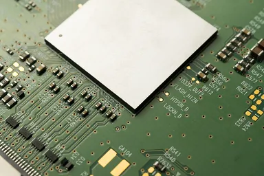
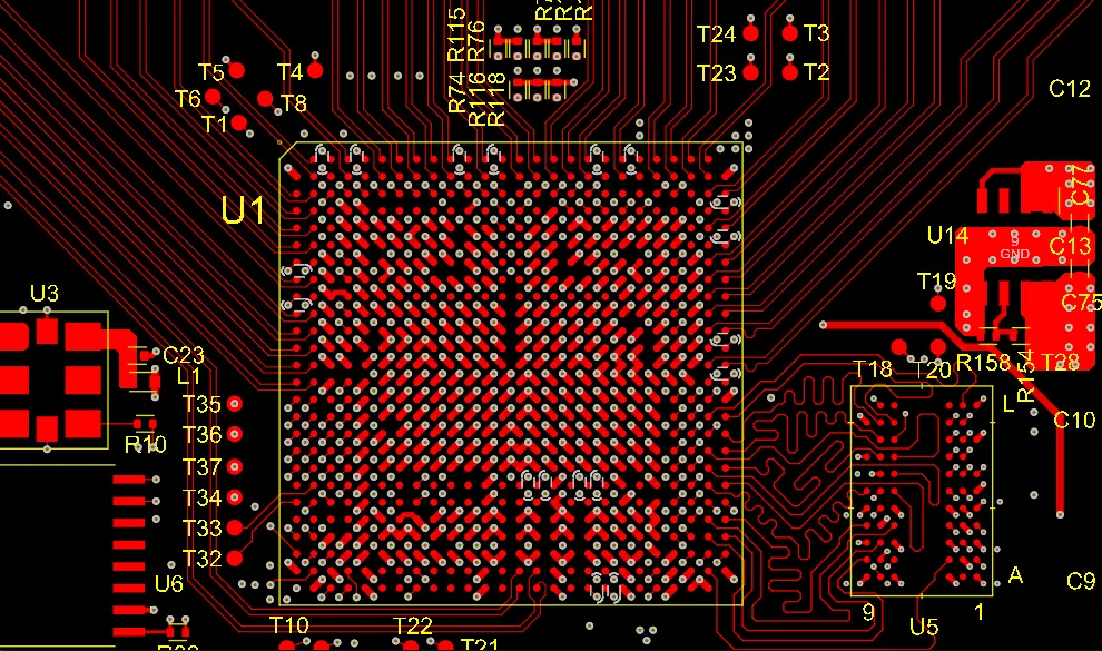
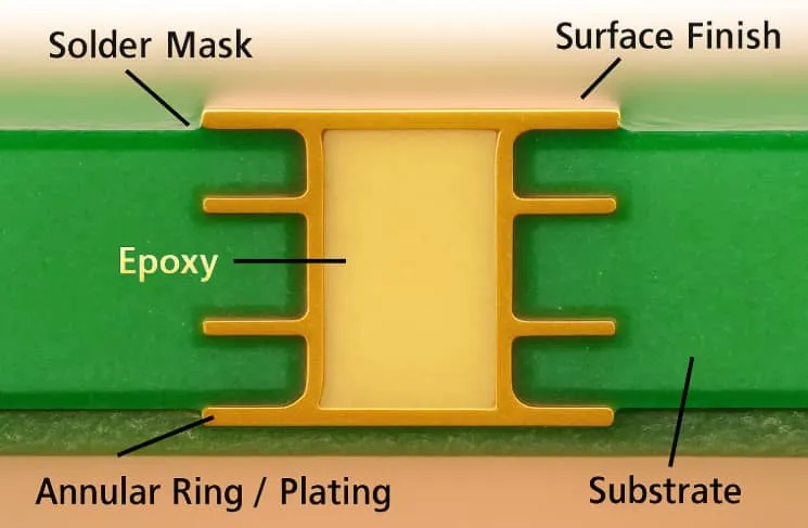
In production we treat HDI microvia solder mask as a registration-and-opening problem first, not a design preference. CAM engineers open the solder mask data with a fixed expansion rule—usually +50 µm to +75 µm on the microvia diameter—then apply a panel-level registration compensation based on the measured shrinkage of that particular material lot. Any microvia that sits inside a BGA or fine-pitch pad array is forced into a non-tented, fully opened condition; we do not allow partial coverage. The mask is exposed on LDI equipment so the absolute registration error stays inside ±25 µm. That is the baseline we run every HDI panel against before the job is released to the coating line.
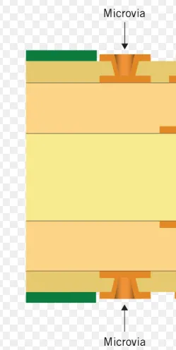
Where the mask wall starts to walk relative to the laser-drilled hole
The issue shows up because the laser-drilled microvia is formed on the inner-layer stack long before the outer solder mask is applied. By the time the panel reaches the coating station it has already gone through lamination, copper plating, and at least one thermal cycle. Dimensional change between the laser drill reference and the final outer-layer artwork is typically 0.03–0.08 % depending on the resin system and the copper balance. On a 500 mm panel that already equals 150–400 µm of cumulative shift. Solder-mask registration on conventional contact exposure cannot hold better than ±50 µm; even LDI drifts ±20–30 µm once the panel is coated and the ink is still soft. When a 100 µm microvia is sitting next to a 200 µm pad, that registration window is enough to push the mask edge onto the via copper or to leave a thin bridge of ink across the opening.
Material behavior adds another variable. High-Tg or low-CTE cores expand less, but the solder-mask ink itself shrinks during the final UV cure. If the development process leaves residual ink inside the microvia, the subsequent thermal shock of reflow can crack that residual film and create a path for ionic contamination. None of these effects are visible in the Gerber data; they only appear once the panel is in the process flow.
What shows up on the finished board when the opening is left uncontrolled
If the solder-mask opening is too tight, the microvia copper is either fully tented or left with a partial covering of ink. In assembly the solder paste cannot wet the via barrel, so the joint volume is insufficient. On fine-pitch BGAs this appears as open joints or intermittent resistance after thermal cycling. When the mask edge sits on the via copper, the exposed copper ring oxidizes during the days between fabrication and assembly; the oxide layer reduces wetting and raises the risk of voiding under the ball.
The opposite error—oversize opening or mask shift toward an adjacent pad—creates a solder-mask bridge thinner than 50 µm. During wave or reflow that bridge can break and allow solder to migrate, producing shorts between the microvia and the neighboring pad. On HDI boards with 0.4 mm pitch the clearance is already marginal; one bridge failure is enough to scrap the entire panel. Yield drop in these cases is usually 3–8 % on the first article, and the boards that do ship often fail customer ICT because of elevated leakage currents.
Rework is limited. Once the mask is cured, laser ablation of residual ink inside a 100 µm hole is possible but slow and risks damaging the copper. Most factories simply scrap the panel rather than attempt selective repair.
How the CAM and process teams actually keep the openings clean
On the CAM side the first filter is a clearance rule set. Every microvia diameter is measured from the drill file; the solder-mask opening is then forced to be at least 100 µm larger than the finished via diameter after plating. For a 75 µm laser hole that finishes at roughly 95 µm after copper, the mask opening is set to 200 µm minimum. Pads that share the same copper feature as the microvia (via-in-pad) receive a non-solder-mask-defined treatment so the copper pad itself defines the land; the mask is pulled back an additional 25 µm beyond the pad edge.
Registration compensation is applied next. We measure the actual panel stretch after outer-layer etch on the first piece of the lot, feed the X/Y scale factors into the LDI job, and re-expose the mask with that correction. For boards with copper imbalance greater than 30 % we also add a local artwork stretch in the CAM data before plotting. The minimum solder-mask dam between a microvia opening and any adjacent copper feature is held at 75 µm after compensation; anything tighter is flagged and either the customer is asked for a redesign or the feature is converted to a filled-and-capped microvia so the mask can sit continuously over it.
Process control on the coating line is equally tight. Ink thickness is kept between 20–30 µm dry; thicker ink increases the chance of incomplete development inside the microvia. Development chemistry is monitored for carbonate concentration every two hours, and the spray pressure is raised 0.2 bar specifically for panels that contain HDI microvias. After development an AOI system inspects every microvia opening for residual ink; any residual larger than 30 µm diameter triggers a re-develop or scrap decision before the panel reaches the final cure oven.
For via-in-pad constructions we require the microvia to be copper-filled and planarized before solder-mask coating. The planarized surface removes the topography that would otherwise trap ink, so the opening can be controlled by the artwork alone. This step is non-negotiable on any board that will see 0.4 mm pitch or finer.

When the factory will relax the opening rules
Relaxation is allowed only when the microvia is purely a thermal or stitching via and sits more than 0.5 mm away from any SMT pad. In those cases a 50 µm expansion is accepted and partial tenting is permitted if the customer explicitly accepts the risk of incomplete solder fill. Boards built on very low-CTE materials with measured panel stretch below 0.02 % can also run with reduced compensation, but the AOI residual-ink check remains mandatory. For prototype quantities under ten panels we sometimes accept a customer-supplied LDI file that already contains the expanded openings, provided the customer signs off that they own the registration risk. In volume production the full rule set stays in force; the cost of a single shorted BGA is higher than the extra CAM time.
The practical limit is density. Once the average microvia-to-pad clearance drops below 100 µm after compensation, no amount of process control can guarantee zero bridges. At that point the only reliable path is to fill the microvias and cover them completely, removing the solder-mask opening from the equation. That decision is made at the DFM review, not on the production floor.