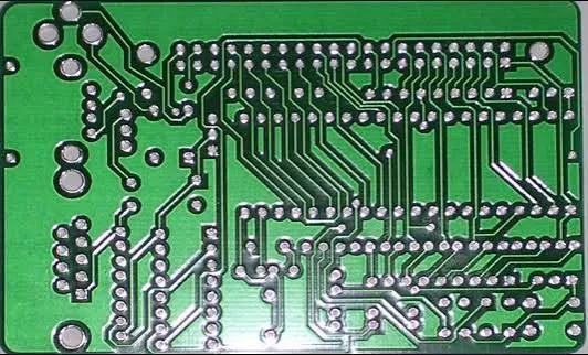
In HDI layouts, the temptation to squeeze every last mil of space is constant. You need to hit that BGA escape routing or pack more fine-pitch devices. But pushing solder mask bridges too thin creates headaches that show up in fabrication and assembly. HDI solder mask bridge design requires respecting the practical limits of the mask process, especially when feature sizes drop below standard.
The Real Pressure in HDI Routing
HDI boards push pad-to-pad spacing tighter than conventional PCBs. Designers often reduce the solder mask web between pads to maintain copper clearance for traces or vias. It feels like a safe trade-off during layout. The mask is just protective coating, right?
Reality hits when the board goes to fab. Liquid photoimageable solder mask has registration tolerances and adhesion limits. In high-density areas, small bridges become fragile. I've seen files where the intended 2-3 mil web ends up marginal or broken after processing.

Why Small Bridges Fail in Manufacturing
Solder mask application involves coating, exposure, development, and curing. Each step introduces variability. For HDI with microvias and fine lines, fabricators often use LDI (laser direct imaging) for better registration, but even that has limits on minimum reliable dam width.
A bridge below 3-4 mils risks thinning during development or undercutting at the edges. The mask can peel or crack under thermal stress in reflow. Copper thickness and surface roughness in HDI builds make adhesion trickier too.
Standard guideline from many shops: aim for at least 4 mil (0.1mm) solder mask bridge for green LPI on typical HDI. Some advanced processes push lower, but yield drops. Don't assume your vendor can hold 2 mils consistently across the panel.
Pad Spacing Decisions That Create Problems
Engineers set pad sizes based on component datasheets and IPC-7351, then adjust mask expansion. For fine pitch like 0.4mm or 0.5mm, it's easy to end up with less than 3 mils of mask web after accounting for expansion on both sides.
The logic is usually "maximize copper for better soldering." But when mask expansion is aggressive to expose more pad, the remaining bridge shrinks. In HDI, where layers are thin and traces route between pads on inner layers, this compounds.

Assembly and Reliability Risks
During stencil printing and reflow, insufficient mask dams allow solder to flow between pads. Shorts become common on fine-pitch BGAs and QFNs. Even if no immediate short, flux residue traps or weak insulation leads to electrochemical migration over time.
Thermal cycling in HDI boards stresses these fragile bridges. The mask can delaminate, exposing copper to oxidation or dendritic growth. In harsh environments, this accelerates failure.
I've reviewed boards where small bridges survived fab but failed in ICT or flying probe due to probe damage on weakened mask.
Minimum Capabilities and Vendor Differences
Not every fab treats HDI solder mask the same. Standard capability often sits at 4-5 mil minimum web. High-end HDI lines with LDI and better materials can hold 3 mil reliably, sometimes lower. Always check the specific vendor DFM rules before finalizing layout.
White oil (solder mask) bridge restrictions become the bottleneck more than copper features in many HDI designs. The outline mentions pad spacing and minimum bridge ability for good reason.

Better Design Choices for HDI Solder Mask Bridge Design
Start by defining mask expansion conservatively: 2-3 mils per side for fine pitch in HDI. This leaves room for the bridge. For critical areas, consider non-solder mask defined (NSMD) pads where appropriate, but verify solder joint reliability.
Gang mask openings for very tight pitches when a reliable single bridge isn't feasible. This eliminates the weak web entirely but requires stencil design adjustments to control solder volume.
Route traces on inner layers aggressively in HDI to free up surface space. Use via-in-pad if the process supports it, reducing the need for tight surface pad clusters.
Numerical Guidelines Worth Following
- For 0.5mm pitch: Target ≥4 mil mask web
- For 0.4mm pitch: Confirm vendor can hold 3 mil minimum
- Mask expansion: 2-3 mil per side typical for HDI fine pitch
- Always add 1-2 mil tolerance buffer in your rules
These aren't absolute but come from repeated DFM feedback. IPC recommendations align closely, emphasizing manufacturable dams to prevent bridging.
Long-Term Field Performance
Weak solder mask bridges don't always fail in assembly. Some pass testing but show issues after months in the field — especially with humidity or temperature swings. Exposed areas from damaged bridges corrode. Solder balls or shorts appear intermittently.
In HDI, where cost and density drive decisions, the reliability margin is already thinner. Don't shave it further with marginal mask features.
Practical Review Steps Before Release
Run DRC with your fabricator's specific solder mask rules loaded. Visualize the mask layer separately — don't trust the default view. Measure the actual web widths in tight areas.
Discuss with the CAM engineer early. They spot where small bridges will cause issues based on their process. Adjust pad sizes or use mask-defined pads strategically.
For HDI solder mask bridge design, the goal is balance: enough space for reliable mask but still dense enough for function. Cutting corners here usually costs more in respins or field returns.
Next time you're tempted to drop that bridge width to fit one more trace, step back and calculate the real impact. Strong DFM on solder mask pays off in smoother builds and better reliability.